
I feel nostalgic over PLCC ROMs. They are by far the most practical way to store firmware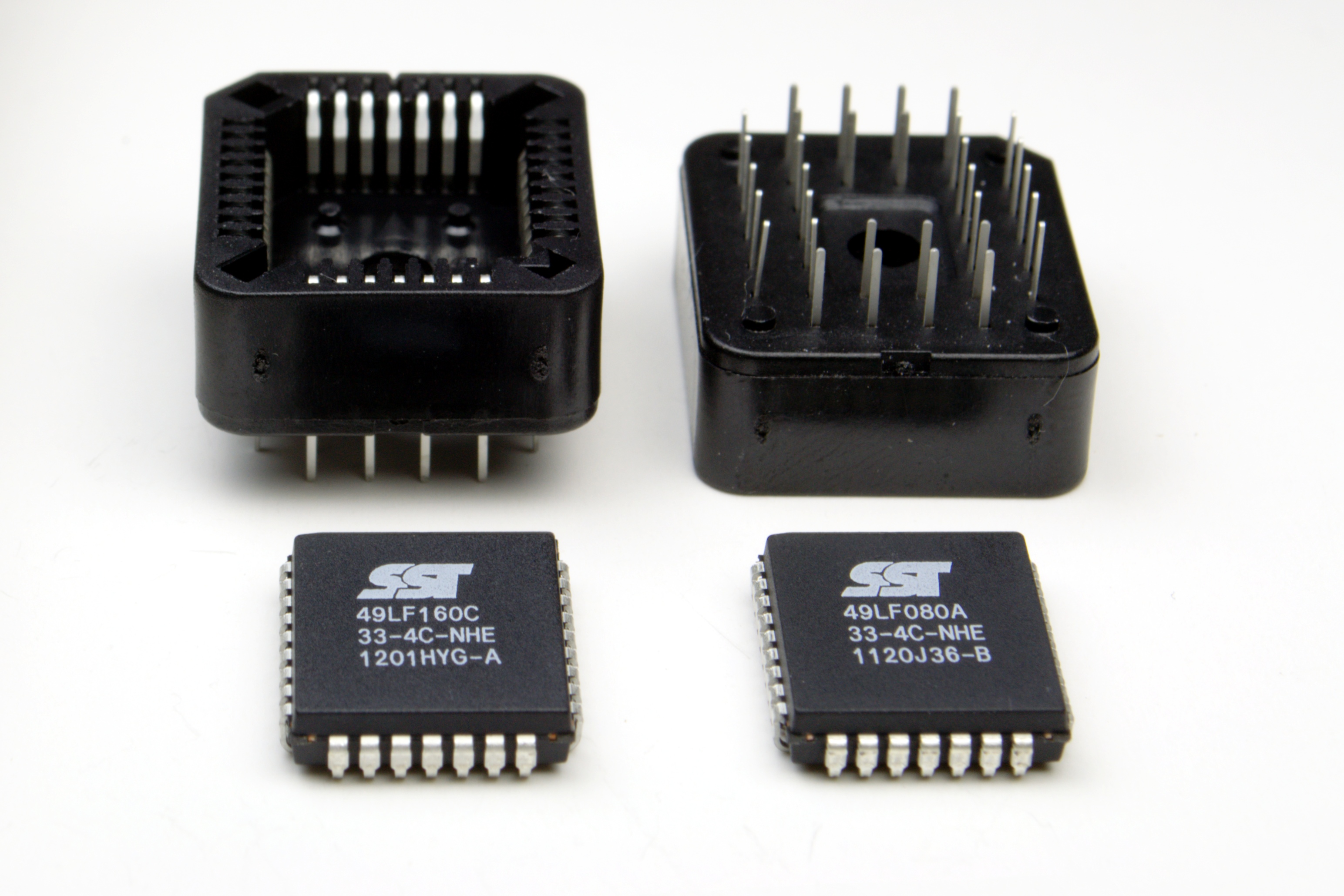 . They replaced the huge 32-pin DIP chips whose pins were very likely to bend or break off as one tried to remove them from the socket. The first board I ever tried to hack on had a PLCC32. After I bricked the board, a friend was able to track down Cristi Măgherușan in Cluj. When I went to meet Cristi in the hope that he might be able to salvage the board, I carried the chip in a little plastic bag in my pocket. He was never able to flash it, but this little detail is of less importance. What matters is that LPC interfaces were most popular in PLCC32 chips, and this is the interface I will be primarily focusing on.
Why bother with LPC in the first place?
Parallel buses were the norm in the 80’s and 90’s. The idea is simple. Have a number of data lines, usually 8, 16, or 32, a clock, and maybe handshake signals. When I say the idea is simple, I mean it literally: the hardware is very simple. The clock is fed straight to the flip-flops which latch the data on the bus. The handshake signals also feed straight into logic gates that control the state of the pins (inputs, or outputs), etc. There is no extra logic needed to figure out when to do what on the bus. Having simple buses saved a lot of silicon real estate for the intended purpose of an integrated circuit.
As transistors got smaller, they got faster, but the laws of Physics did not change. Electromagnetic waves in a metal travel at the speed of light (well, a little slower when you consider electrodynamics effects). Since the information is carried on the wavefronts, we really don’t care how fast electrons are moving. If a signal is 10 centimeters longer, it will arrive 0.33 nanoseconds later. On an 8MHz ISA bus (125ns cycle time), this delay is insignificant. The little physics policemen do not stop here, however. Wires are nothing but little series inductors radiating energy to ground planes and other wires like little parallel capacitors. It takes tiny amounts of energy to energize a wire to the right voltage. This process takes a tiny amount of time, usually a few nanoseconds. If we’re lenient, and allow 12ns , add the travel time to our sloppily routed signal, and it takes 12.33 ns from the time we drive the signal to the time it reaches its destination at the correct voltage. That’s 1/10th of our ISA cycle time. To get around this, simple buses drive the data on one edge of the clock, and sample it on the other edge.
Fast-forward to the 90’s and the 33MHz PCI bus. If we allowed 12 ns for any signal to rise, and 12 ns for it to fall, we would already waste 24 ns of the 33 ns allotted for each cycle. We get a tiny 5 ns window to latch the correct data. All of a sudden, routing signals to reduce inductance and capacitance, and match their travel times becomes a lot more important… and expensive. ISA is downgraded to a second-class citizen: It doesn’t make sense to route a high number of additional signals for a low-speed bus, and it doesn’t make sense for low-speed components to move to more expensive PCI silicon. This is the gap the LPC bus fills.
The LPC
LPC eradicates ISA for a 4-bit, 33MHz bus, a clock, and a handshake signal. The 33MHz clock is not an accident. Rather it is meant to be derived directly from the PCI clock. The signaling bandwidth of 16.5 MB/s (33MHz * 0.5 Bytes) is very close to ISA’s 16MB/s (8MHz * 2 Bytes). Handshakes are handled through the data pins, though they require very little silicon logic.
Let’s have a look at what LPC brings us:
- LAD[3:0] – 4-bit data
- LCLK – 33MHz clock
- #LFRAME – Start of frame handshake
Signaling and handshakes happen within a frame. A frame is a predefined sequence of handshakes and data transfers. Somewhere within the frame we transfer the actual data byte. Let’s take a look at what a typical frame looks like: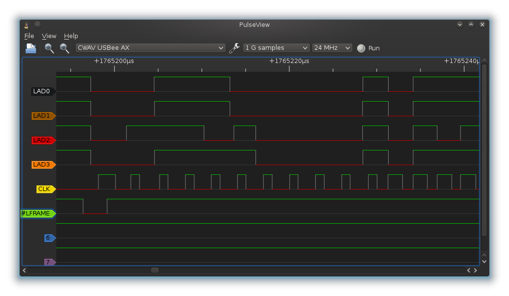
A bit cryptic until we put some meaning into the signaling:

Aaah! Much better. Here’s what happens:
- #LFRAME starts a new frame.
- LAD is at 0x0, which indicates the start of a cycle for a target.
- In the next cycle, we put 0x4 on the LAD pins. This indicates we want to start a memory read.
- The next 8 cycles are the memory address: 0xFFBC0000. This is the JEDEC address for reading the manufacturer ID.
- Next, we start a turnaround cycle (TAR) which transfers the control of the bus to the target.
The TAR cycle is supposed to last two clocks. We drive the pins high during the first clock, then float them with a pull-up in the next clock. The chip is supposed to wait until the third clock to send us a SYNC (LAD[3:0] driven low). And the first problem: the SST 49LF080A is guilty of violating the LPC spec. It does not wait for the third clock to send the SYNC. It most likely implements an internal delay, and completely ignores the TAR cycle. It’s these sort of unexpected problems that have prompted me allocated a lot of time in my GSoC project to figuring out how to master the LPC bus. This problem will most likely require ARM assembly blackmagic to more closely match the timing to that of a 33MHz clock.
After the skipped clock, everything looks fine though (If one clock early can really be considered “fine”). We get 0xBF in the data cycle, which is SST’s manufacturer ID. Success!