
GSoC 2022 coding period is about to come to an end this week. It has been an enriching 12 weeks of reading old code, designing algorithms and structures, coding, testing, and hanging out over IRC! I’d like to take this opportunity to present my work and details on how it has impacted Flashrom. 🙂
You can find the complete list of commits I made during GSoC with this gerrit query. Some of the patches aren’t currently merged and are under review. In any case, you are most welcome to join the review (which will likely be very helpful for me).
Definitions
Let me clarify some terminologies used hereafter
- Region: A list of contiguous addresses on the chip
- Layout: List of regions
- Locked region: There are some regions on the chip that cannot be accessed directly or in some cases cannot be accessed at all.
- Page: The entire flash memory is divided into uniform pages that can be written on. You have to write on an entire page at once.
- Erase block/sector: According to each erase function, flash memory is divided into regions (not necessarily uniform sized) that can be erased. You have to erase an entire erase block at once. So each erase function has a different erase block layout.
- Sub-block: An erase block is a sub-block of another erase block if it is completely inside the latter.
- Homogenous erase layout: All erase blocks in a layout are of uniform size.
- Nonhomogenous erase layout: There might be erase blocks of varying sizes in this layout.
Need for this project
To change any 0 to a 1 in the contents of a NOR-flash chip, a full block of data needs to be erased. So to change a single byte, it is sometimes required to erase a whole block, which we’ll call erase overhead. Most flash chips support multiple erase-block sizes. Flashrom keeps a list of these sizes and ranges for each supported flash chip and maps them to internal erase functions. Most of these lists were sorted by ascending size. I added a simple test to ensure this and corrected the ones which gave errors.
Earlier, Flashrom tried all available erase functions for a flash chip during writes. Usually, only the first function was used, but if anything went wrong on the wire, or the programmer rejected a function, it falls back to the next. As the functions are sorted by size, this results in a minimum erase overhead.
However, if big portions of the flash contents are re-written, using the smallest erase block size results in transaction overhead, and also erasing bigger blocks at once often results in shorter erase times inside the flash chip.
So in a nutshell, the erase function selection in Flashrom was sequential, i.e. they started from the function with the smallest erase block and moved to the next one only in case of an error. This was inefficient in cases where bigger chunks of the flash had to be erased.
Current implementation
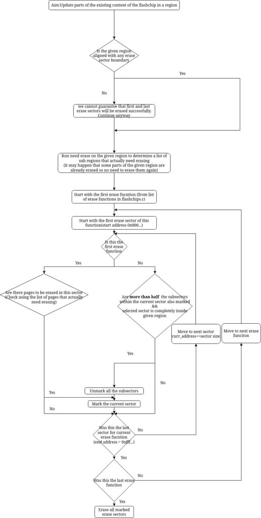
After rigorous discussion with my mentors and with the community, we decided on a look-ahead algorithm for selecting the erase functions or the erase blocks to be more precise. From the layout of erase blocks as seen by different erase functions, we make an optimal selection.
We start with the first erase function (remember this erase function has the smallest erase blocks) and mark those blocks which lie completely inside the region to be erased. Then moving on to subsequent erase layouts and marking those erase blocks that have more than half of the sub-blocks marked and then unmarking the marked sub-blocks. Finally, erase all the marked erase blocks. This strategy ensures that if we have a large contiguous region to be erased then we would use an appropriately large erase function to erase it.
The above-mentioned strategy had some challenges and required a few tweaks:
- The region to be erased may not be aligned to any erase blocks. This could be easily overcome by extending the ‘to be erased’ region to align it with some erase block.
- The above solution of extending the region brought a new challenge – the newly aligned region might overlap with write-protected regions. In this case, the erase function would fail to erase the erase block containing this region.
- It may happen that some erase functions are not supported by the programmer. This would lead to catastrophic failure. To this end, we thought of first getting a list of erase functions supported by the programmer and then running the algorithm on this subset of erase functions.
So with this, we were all set to begin the implementation of the algorithm. Or so I thought. Flashrom had stored information regarding the erase layout in a nested format which was very difficult to use so I had to flatten them out and fit them in a data structure that would give me quick information about sub-blocks as well. 😮💨
For a better understanding of the algorithm, I made the following flowchart.
Testing
Testing on hardware is difficult because you need all the different chips and programmers and test on each one of them to be sure that your code is working correctly. On top of that, identifying all possible scenarios adds to the burden. This definitely takes a lot of time and effort and my mentors and the community is helping a lot with it.
The current progress of testing can be seen here. Feel free to suggest more cases and help with the testing. It will definitely help a lot.
Future work
Definitely, the code or algorithm isn’t fully optimized and can be improved further. Also one can fix the progress bar feature to Flashrom, which got broken due to my code😅.
Acknowledgments
I’d like to thank Thomas Heijligen and Simon Buhrow for being excellent mentors, Nico for providing constant code reviews and giving regular inputs, and everyone in the Flashrom community for being helpful and friendly.