CCCamp 2015

We had an table on the cccamp 2015 in Mildenberg. The cccamp (chaos communication camp) is one of Europe big hacker events every 4 years where several hackers come together and do camping. Everybody could relax a little bit and talk to each other in a nice background. The camp infrastructure contained own wifi, dect, gsm network and a 10 GBit uplink in the middle of nowhere. You could give your tent a 1 Gbit uplink to the internet ;).

Our table was in the BER village, named to the never finished airport near Berlin, Germany. Several people from the coreboot community showed up (CareBear, felix, mue, paulk-collins, tnias, zaolin, […]) and we shared a lot of ideas to each other. In that way we flashed several laptops, replaced some WSON chips with SOIC-8’s. Also we’ve found another bug in the sandybridge ram init, a fix is waiting for merge on gerrit #11248.
paulk-collins came by to talk about a EC open source firmware for the ENE KBxxx embedded controllers.
One of the MAME hackers visited us to get ideas how to port a Dell notebook (ENE KBxxx based EC).
Felix did some work on ME as well other hackers joined him.
Tnias and zaolin started the idea of a raspberry pi doing all the flashing including detection of the device. This could let us drink more Mate while other do the flashing themself.
In the end a thunderstorm reached our tent and we had to evacuate it.

Hopefully everybody can come to Bonn this year.

[GSoC] EC/H8S firmware week #7|#8

Week #7 was is little bit frustrating, because of no real progress, only more unfinished things which aren’t working. Week #8 was a lot better.

1. Sniffing the communication between the 2 embedded controllers H8S and PMH4.

I’ve tried to build an protocol analyser with the msp430, but the data output was somehow strange. For testing purpose I used my H8S firmware to produce testing data. But the msp430 decoded only wrong data. I’m using IRQs on the clock to do the magic and writing it to a buffer before transmitting it via UART. Maybe the msp430 is too slow for that? Possible. Set a GPIO to high when the IRQ routing start and to low when it ends. Visualize the clock signal and connect the  IRQ measure pin to an oscilloscope. The msp430 is far too slow. I’m using memory dereference in the IRQ routine, which takes a lot of time. Maybe the msp430 is fast enough, when using asm routine and registers to buffer the 3 byte transmission. But a logic analyser would definitely work. So I borrowed two logic analyser. An OLS (Openbench Logic Sniffer) and a Saleae Logic16.

There isn’t so much data on the lines. Every 50 ms there is a short transmission of 3 byte. But I don’t want to decode the data by hand. So it needs a decoder for the logic analyser. sigrok looks like the best start point and both analyser are supported.

I’ve started with the Openbench Logic Sniffer, but unfortunately it doesn’t have enough RAM to buffer the input long enough. Maybe the external trigger input can be used. But before doing additional things I would like to test with the Logic16.

The Logic16 doesn’t support any triggers but it can stream all data over USB even with multiple MHz. Good enough to capture all data. I found out that the best samplerate is 2 MHz. Otherwise the LE signal isn’t captured, because it’s a lot shorter than a clock change. In the end I created a decoder with libsigrokdecode.

sigrok-cli -i boots_and_shutdown_later_because_too_hot.sr –channels 0-3 -P ec_xp:clk=2:data=3:le=1:oe=0 | uniq -c 

67 0x01 0x07 0xc8
3 0x01 0x04 0xc8 
4 0x01 0x10 0x48
1120 0x01 0x17 0x48
67 0x01 0x07 0xc8

0x01 0x07 0xc8 is called when only power is plugged in, like a watchdog(every 500ms)
0x01 0x17 0x48 is called when the device is powered on, like a watchdog (every 50ms)
0x01 0x04 0xc8 around the time power button pressed
0x01 0x10 0x48 around the time power button pressed

2. Flash back the OEM H8S firmare

The OEM H8S firmware is included in the bios updates. cabextract and strings is enough for extracting it out of the update. Look for SREC lines. Put the SREC lines into a separate file and flash them back via UART bootloader and the renesas flash tool. The display powers up and it’s booting again with OEM BIOS.
I could imagine they are using a similar update method like the UART bootloader. First transfer a flasher application into RAM and afterwards communicate with the flasher to transfer the new firmware, but the communication works over LPC instead of UART.

3. Progress on the bootloader

I’ve implemented the ADC converter to enable the speaker amp and the display backlight brightness.

Written down LPC registers and just enable the Interface in order to get GateA20 working. Still unclear how far this works.

4. How to break into the bootloader?

The idea of the bootloader is providing a brick free environment for further development. The bootloader loads the application which adds full support for everything. It should be possible to stop the loading application and flash a new application into the EC flash. When starting development on the x60 or x201 I want to use I2C line as debug interface. I2C chips have a big footstep and are easy to access. But there must be a way to abort the loading. I will use the function key in combination with the leds.

  1. Remove the battery and power plug.
  2. Press the function key
  3. Put the power plug in
  4. Wait until leds blinking
  5. release the function key within 5 seconds after the leds starting to blink to enter the bootloader.

The H8S will become I2C slave on a specific address.

What next?

  • Add new PMH4 commands to the H8S
  • solder additional pins to MAINOFF PWRSW_H8 A20 KBRC
  • use the logic analyser to put the communication in relation with these signals
  • UART shell
  • I2C master & client
  • solder LPC pins to analyse firmware update process
  • test T40 board with new PMH4 commands and look if all power rails are on

[GSoC] EC/H8S firmware week #6

This week I looked at the communication between the EC H8S and the PMH4. The PMH4 (likely power management hub) is an ASIC which takes care of the power control. It controls who get’s power and who not. It doesn’t do any high level work, more like a big logic gatter. The PMH4 has inputs from several power good pins from different power rails and chips. On the output side it controls some power rails. It can also reset the H8S. The PMH4 also knows over some pins in which power state (ACPI S0,S4,S5) the board is. It doesn’t do any high level work. It’s more like a big logic gatter. There are no ADC on any power lines.

The PMH4 is connected to the H8S via 4 Pins. ~OE LE DATA CLK.

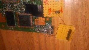
gsoc 2015 pmh4 connector t40

I connected a buspirate in SPI sniffer mode to debug the protocol. But the output looked a little bit strange. There was no data from the PMH4 to H8S (MISO) and the data comes in burst. To get more knowledge on the protocol I used a digital oscilloscope.

pmh4 oscilloscope

The protocol doesn’t look like SPI. LE get’s low after every transmission, ~OE is just high, clock and data just transfer the data. Sometimes when the H8S gets an interupt the Clock pause for some time and continues with the data afterwards. The clock is around ~400kHz.

I confirmed the protocol via the oscilloscope, but still I don’t get any sign from the board. No fan, nothing else. There must be more than this single transmisison. Maybe the board is to much damaged. My modified board was already broken when I got it. There is a loose connection related to the cardbus. Maybe this is my problem I don’t know.

I’ve two board with two connectors for the PMH4 here. Why not using the OEM one as starter help for the other one?

t42 gives some starting help

I think the PMH4 does what it should do. The H8S has an digital-analog-converter pin connected to the video brightness. But I haven’t implemented it yet. But I don’t think the device booted, because neither the CPU nor the chipset produce any heat. Ok, maybe it does, I only used my finger as thermometer. A thermal camera would help here. I’ll borrow a thermal camera for that.

There are lot of pins which I ignore atm. E.g. A20 pin. Is there something to do in a specific time serie?

What’s next?

  • build a small protocol sniffer for the PMH4 XP using a msp430 or stellaris arm
  • make progress on the bootloader
  • find a way to flash back the OEM H8S firmware
  • find a way to flash my bootloader via OEM flash tools

My requirements to the bootloader are

  • UART flashing via XMODEM
  • a simple UART shell
  • I2C as recovery and shell as well

I2C pins are a lot easier to find and modify than the H8S UART. I’m not yet sure if the H8S should be the master or the slave and on what address he should use? Multiple? UART tx is working. Rx is a task to do.

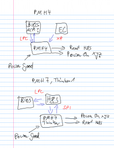
PMH4 / PMH7 / Thinker communication

On newer board the PMH interfaces changed (>= x60, t60, …). They merge the LPC interface and the XP interface into an protocol over SPI. And the new PMH is used as GPIO expander as well.

pmh4 pmh7 thinker communication


[GSoC] EC/H8S firmware week #5

The T40 is flashing leds! The toolchain is still a little bit tricky. I’m using the debian package gcc-h8300-hms, written a small linker script and took the startup assembly routine from Johann Gysin’s led radiator.

Now I can flash leds. But what about booting the board? I would say it’s enough to put

  • (!MAINOFF) = high
  • FAN ON = high
  • pulse high on (!PWRSW_H8)

But it’s not enough. Also the FAN isn’t starting to rotate. I’ll try to debug every pin this week and solder some debug pins for the 2nd EC (PMHx) to the my modified T40 as well as to an unmodified T42p. The H8S is talking to the PMHx via SPI, while the H8S is the master and is doing bit banging SPI in software, because it doesn’t have a hardware unit for that. I’ll also use these pins for testing my SPI implementation. I’ll try to reuse an open source SPI implementation.

I also asked me if it’s a good idea to port coreboot for the T40 before continuing any efforts to the EC, but it’s a little bit harder, because the T40 uses a LPC/FWH flash in a TSOP40 case. Another option is changing the hardware to a board which is already supported by coreboot like a x60/t60 or x201. But it’s much more harder to access the 8 pins for flashing the EC on these boards.

Before switching to another board, the powersequencing must work and I need a robust recovery way, because when you kill the EC by flashing a new firmware, you don’t get a second chance, unless you solder a lot. Chrome EC fix this problem by splitting the EC firmware into 2 parts. One read-only part and one read-write’able part. Only the second part gets updated and the read-only part can at least boots the device.

Before starting the H8S port for Chrome EC I want to have a bootloader. Because it would improve developing speed. I think implement this is much faster than doing the full Chrome EC support and most of the bootloader code can be re-used for Chrome EC.

I’m also not perfectly sure Chrome EC is the best solution. It’s special use-case is EC, which is perfect. But neither the documentation (I think there is more than one page) nor the bugtracker is public. Thus it makes difficult to use. I’m also not sure if Chrome EC would apply my H8S port into their repository.

[GSoC] EC/H8S firmware week #3|4

In the last 2 weeks I managed to flash the H8S on the T40 using the OEM Renesas Flash Tool including their flash application. Flashing works in 2 steps, first upload a flash application into the H8S. Second this flash application will receive the firmware (via serial) and write it into the flash. Thanks to Renesas this application is available in source code. I would like to write an own flasher later.

But I wasn’t able to create a proper application yet. I could write the led programm in assembly, but having a working c compile is needed anyway.

I built a toolchain with gcc 4.9.2. The toolchain buildscript is very simple and can be found on github. I stopped my building efforts for now (building one based on gcc 4.4.6). There’s also a debian package for h8300 (based on gcc 3.4.6) which may be a good alternative. Before continuing in building toolchains and my led application, I’m reading me into linkerscipts and take a look how the compiler is working (e.g. what must a crt0 do?).

At the moment I know how the application should be compiled, where the reset vectors are and where the entrypoint. But putting these things together into a binary image is my task now.

The dev board I mentioned in my last post was stuck by the german post for the last 2 weeks, because there were on strike. The board is now in the custom office and I’ll collect in the next days, which will takes severals hours in Berlin.

[GSoC] EC/H8S firmware week #2

The last week was a little bit depressive. I did the some resoldering. Pin P90 wasn’t connected to 3.3V which is needed to enter the flash boot mode. It was soldered  to the VCC of the Serial level shifter MAX3243. After searching some minutes with the Multimeter for a better power source, I decieded to use 3.3V near the H8S. It’s now a very long cable across the board.

Now let’s see, how good this works? Nothing :(. Recheck with a voltmeter and found another problem with P91 (/SUS_STAT). When connecting SUS_STAT with an 1k resistor to 3.3V the voltmeter shows 0.04V. This means it’s driven by something else to 0V. My hope was that the chipset isn’t driving this until it’s powered. But sadly it is driving it to 0V. What’s SUS_STAT? SUS_STAT can be used as LPCPD (LPC power down) and is used to notify devices to enter a low power state soon. Suspend Status is active low, which means all device should be in low power mode.
What should I do now? I need 3.3V on that line.

There are multiple solution:

  • Remove 1k and burn it to death. But likely this could kill the chipset or
    a least this certain pin or multiple pins
  • Cut the pin
  • Bend the pin upwards while desoldering
  • Desolder the whole chip and bend afterwards, resolder
  • Replace the chip with a socket (expensive and rare)

This decision is not easy to take, especially because I never done most
of these things. This got me stuck for a while until Peter helped me out,
he bend a single pin upwards. Thanks!

The next week milestone is still flashing the EC, the same goal since the first week. So the time schedule will be a little big chaotic. Maybe I can hurry up and reach another weekly goal fast than a week.

Because I was stuck on that a little bit, I took another look on ebay and bought a development board with a H8S/2633. 2633 is a little bit newer than the 2100 series
which is used in Lenovo laptops. The board should arrive in one week, but atm it’s in german customs. Such development boards are hard to get for a “good” price. Brand new boards start with several hundred euros or dollars. E.g. the debugger E10 (USB device) cost around 1000 Euro, it’s only a stupid USB device. I already bought on ebay an E8, previous generation debugger, but it can not debug the chip, only flash them with the Renesas software/IDE.

Beside my project I’ve done some other work on coreboot. I helped Holger Levsen on creating a reproducible build job for coreboot on reproducible.debian.net. More info about reproducible builds are on their wiki page.  To improve reproducibility I created 2 patches #10448 #10449. They cleaned up reproducible bugs in coreboot and without building Payloads, most targets are now reproducible. Great thanks to Holger Levsen for his work on that!

[GSoC] EC/H8S firmware week #1

The first task of my project is a working development board. A development board means that I have serial communication and I can flash new firmwares the chip and whole mainboard isn’t booting. The chip is a H8S 16-bit microcontroller with 64kb to 128kb EEPROM and is available in different packages. BGA and TQFP. BGA means the pins are under the chip, TQFP has pins on the side. TQFP is nice to hack, but most modern Thinkpads use the BGAs. But a T40 or T42 use a TQFP package. A friend donated his old T42 to me! Thanks a lot! Now with a hackable T42 I can start to create a development board out of the T42 mainboard. Like most other microcontroller this chip has a programmable bootloader in a ROM (called rom loader). The bootloader can boot to different states, configurable via 5 pins (MD0 MD1 P90 P91 P92).
P90 to P92 are only read when MD0 and MD1 are in a special bootstate.
After reading the documentation I found that the pins must match the following volatage levels to select the flash boot mode:

MD0-MD1 = 0V, P90-P92 = 3.3V.

Besides these configuration pins we need some additional wires to the following pins:
/RES – reset active low
UART RX – serial communication
UART TX –

Now it gets interesting. The MCU (microcontroller unit) can use a pin for different purposes depending on the PCB designer. Those pins called multifunction pins. Hopefully we don’t get blocked by unaccessible pins. After reading more documentation and using a Multimeter on the board I found out that /RES, RX, TX, MD1 require soldering, but are easy accessible. MD0 is already in a good state.
P90 is connected via a resistor to ground, but we need it to 3.3V.
Let’s find the resistor to solder 3.3V to it… Mhh. tricky! 3h later I found it on the
board hidden under the PMH4 (2nd EC/GPIO expander). Very uncommon.

P91 is named /SUS. Suspended active low, but can be driven by multiple controllers (chipset + h8s).
Because we want to boot linux on the main cpu later in the project we should not kill the chipset. I added a pin connector to this pin.

And the last pin P92 was connected to the SuperIO UART’s level shifter (MAX3242). I had to desolder the chip because P92 was driven by the level shifter.

Near the EC are 2 testpoints which are connected to an I2C bus. I soldered these too, because an I2C could be useful.

1 P91
2 GND
3 md1
4 /RESET
5 RX
6 TX
7 I2C SDA
8 I2C SCL
+
1 patch cable with a 3.3V + 1k Resistor (for P91).

So far so good. But somehow it doesn’t work. Some pins doesn’t have the right level. P92 doesnt have 3.3V. Why not?
P92 is pulled up via a resistor to VCC of the TTL shifter. The VCC isn’t powered. I need to resolder it to another 3.3V pin somewhere and take another look
on the other levels too.

PS. Some work was already done before GSoC started. I posted the first part of soldering on my blog

GSoC 2015 H8S EC firmware

Hi community,

I’m Alexander Couzens on the list and in IRC known as lynxis. I’ve experience with embedded Linux and hardware integration of wireless devices using OpenWrt. I started modifying my vendor BIOS several years ago because my brand new Lenovo X201t didn’t allow me to use good wireless cards because it checked all pci networks devices against a white list. After my mainboard was replaced I had to do the same modification again or install coreboot. Of course I went for coreboot 🙂 While installing coreboot I also started developing it, my GSoC is the H8S Embedded Controller firmware. The EC controls a lot of things in your laptop. An EC controls the battery charging and discharging, the keyboards, docking and undocking, multiple sensors, thermals sensors, fan, lid switch and power regulators.

Continue reading GSoC 2015 H8S EC firmware