
In the last blog post I talked about the test-interface-board. There were some concerns about the use of FT232H chip and extra features like voltage and temperature measurement were not required. Keeping in view all the suggestions and improving things on my side I have redesigned the board.
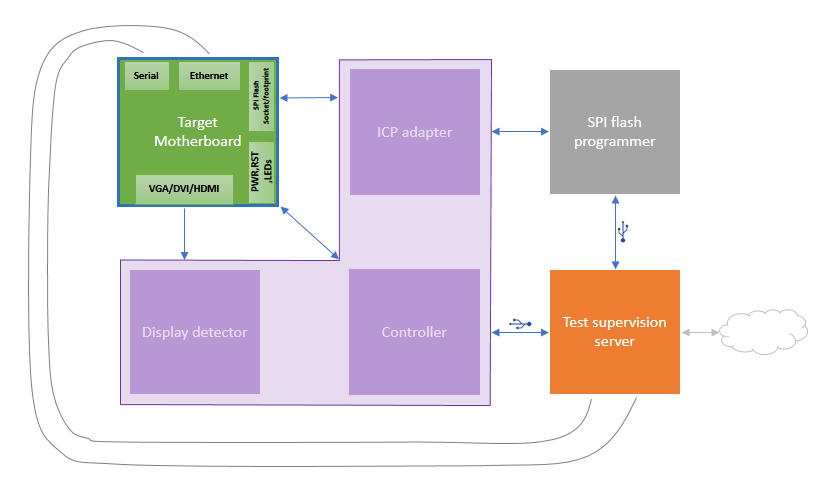
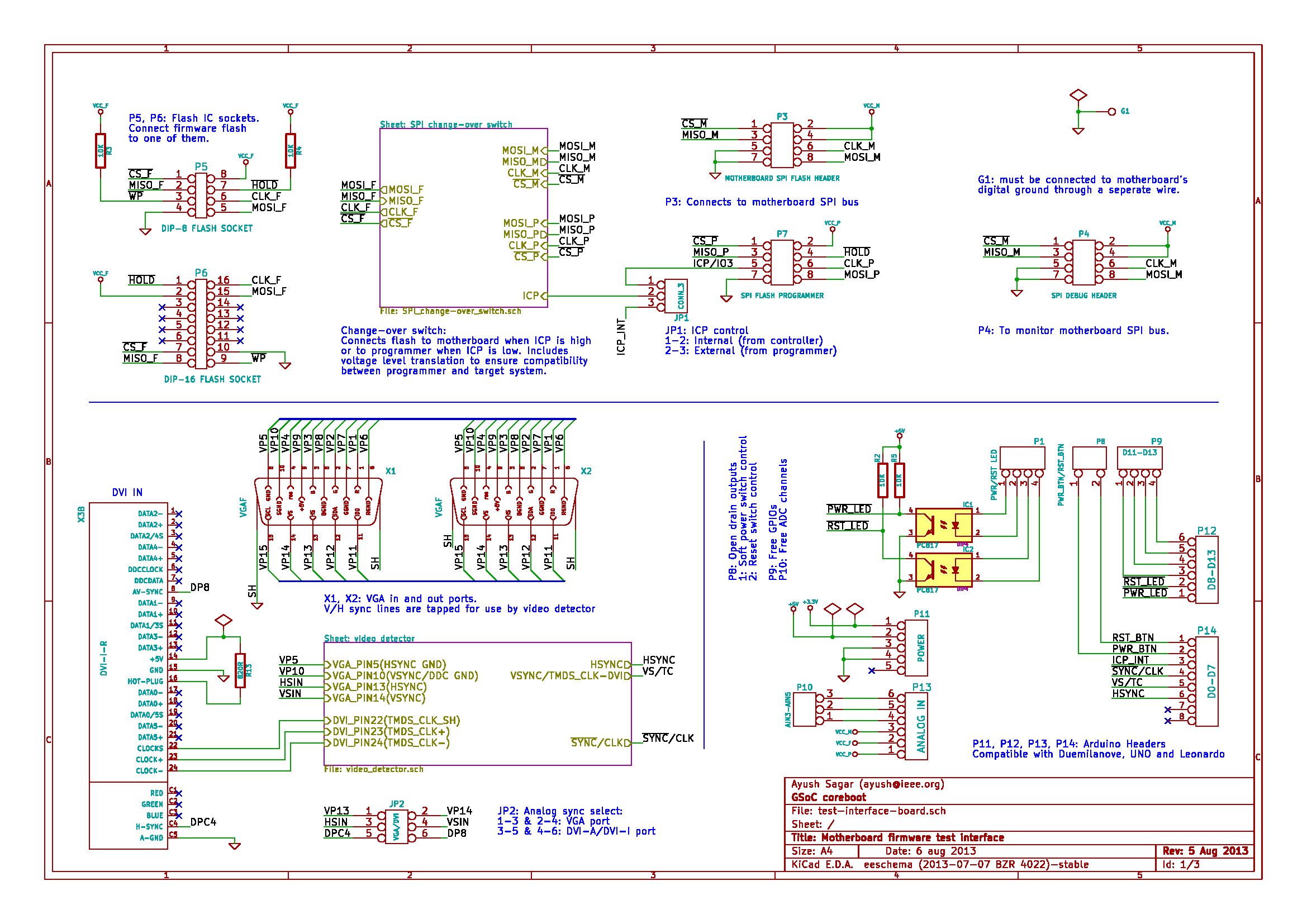
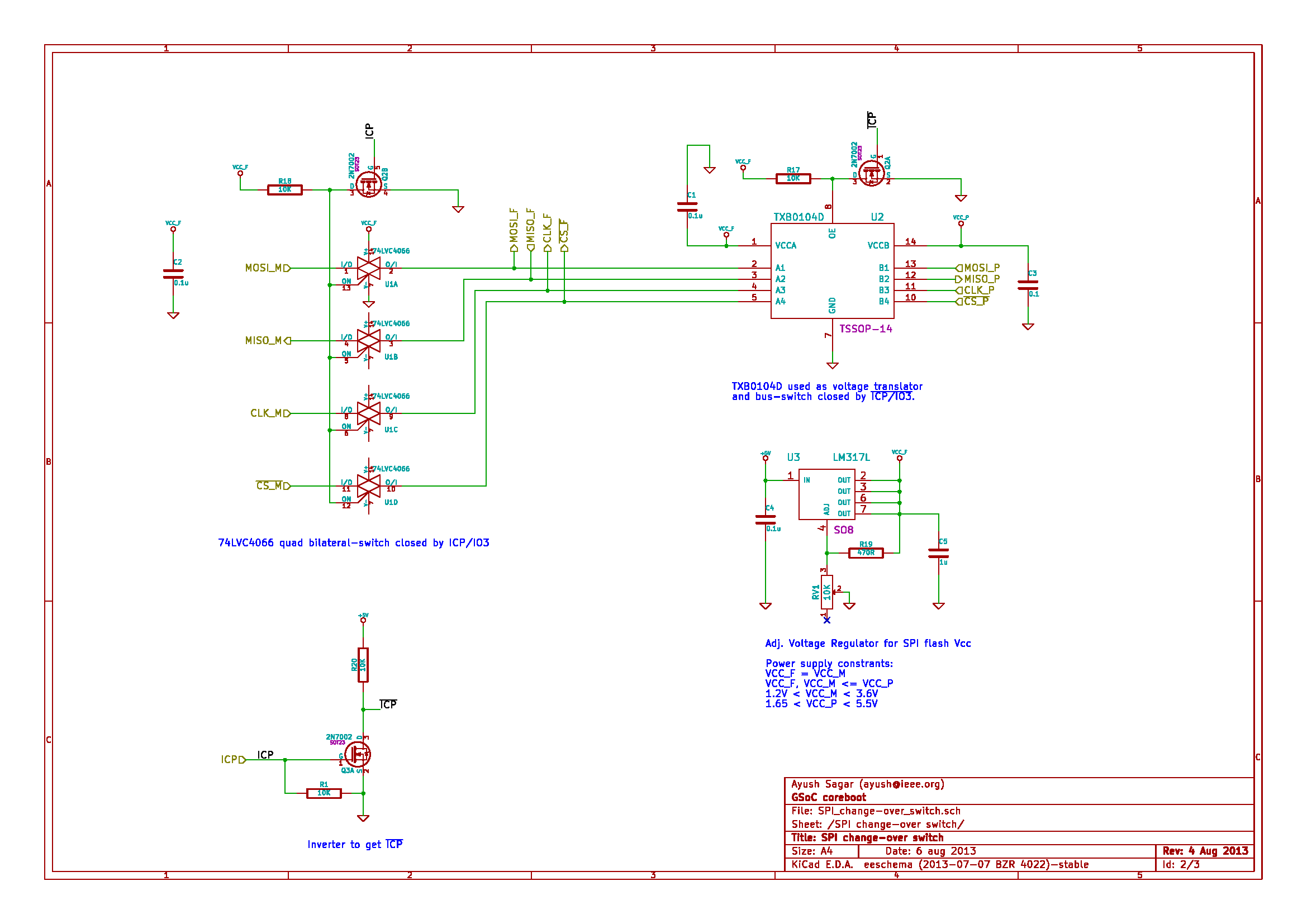
The figure above shows only one target board connected to the test supervision for simplicity. The purple L-block is the test-interface-board. This time, instead of using an integrated flasher I wish to support all existing flashers so I have developed an ICP adapter. An In-Circuit Programming (ICP) adapter contains the firmware flash memory removed from the motherboard and it acts as an electronic change-over switch that connects this flash memory to the motherboard or the programmer as required. It also includes logic-level translation to support as many as possible combinations of programmers and motherboards. The support for programmer voltage is in range 1.2V-5.5V and for motherboard SPI voltage it’s in range 1.65V-3.3V.
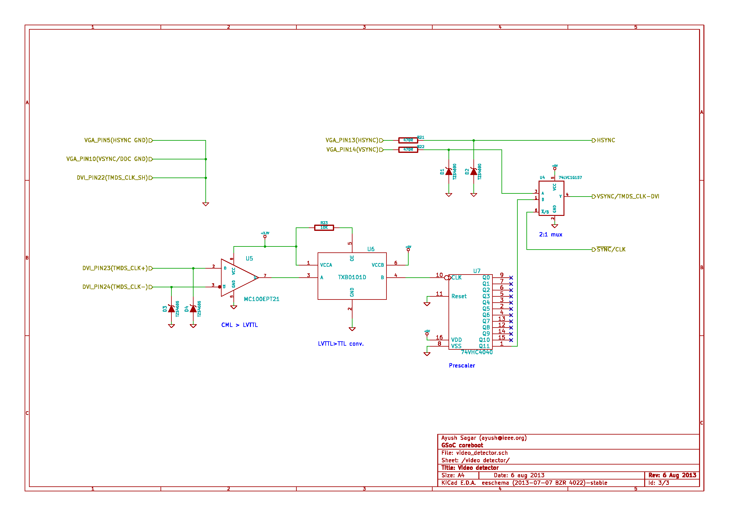
As a quick test for VGA initialization I’ve added video detection for Analog video (VGA), DVI and HDMI ports. This checks presence of signals that are only there when video is active. In other words, it checks whether a monitor’s status led would turn green if it’s plugged to the motherboard without actually plugging one. I have prepared schematics, some parts of which are yet to be validated through prototyping. This will all be implemented as an Arduino add-on board (aka Shield) for convenience and the Arduino would act as the controller.
The Serial and Ethernet ports can be connected in the usual way using Serial-to-USB cables, Ethernet cables and hubs.
Choosing the controller and form factor:
I was initially considering to build this around PIC18F14K50. But later I changed my mind to use an Arduino instead for the following reasons:
- There’s no programmer for this chip except for the official ones like Pickit3. Someone has built a PIC18F programmer (https://sites.google.com/site/thehighspark/arduino-pic18f) that doesn’t support this chip but I can modify it to support this chip, however, testing this would be time consuming.
- The open-source tool-chain for working on this chip appears to be sdcc and gputils. Pinguino, an Arduino like IDE is also there but it doesn’t support this chip. As I’m new to PIC it would be time consuming to work on these. Arduino itself it an open-source platform and has extensive open-source toolkit.
- I was thinking of a single chip solution but later I realized that putting the USB stack and my program on the same chip may not work well.
Although Arduino boards appear to be a bit expensive, they’re really worth the cost as they integrate 3.3V and 5V regulators, DC jack, USB connector, separate USB-UART converter and all the components required by the microcontroller. Even the official Arduino boards are worth the cost because it has good quality components. Arduino Duemilanove, Uno, Leonardo are the inexpensive ones and their clones are common. So the idea is to make the circuit as an add-on board for these Arduino boards.
In-Circuit Programming adapter
Support for in-circuit programming varies among motherboards and most motherboard that I’ve seen don’t seem to support it at all. Connecting a programmer directly using test-clips can risk damaging the motherboard south-bridge chip if it’s not in the high impedance state. So I thought it’s better to design some kind of mediator for the motherboard and the programmer so these two work in harmony. Also, there needs to be a standard procedure for flash programming that can work on all motherboards. So the solution is conceptually simple, and it is to design a changeover switch for connecting the flash chip either to the programmer when firmware update is desired or to the motherboard when normal operation is desired. I also see a possibility of seeing flash chips of lower voltages than 3.3V in future if not now so voltage-level translation is also included. The power source for driving the flash chip comes from the controller and not from the motherboard so that flashing doesn’t depend on the power state of the motherboard. As a result the flash chip voltage (VCCF) needs to be matched to the motherboard SPI bus voltage (VCCM) by carefully adjusting a potentiometer when the system is being set up. In case an ICP header is available in the motherboard and the programmer voltage is compatible then this ICP adapter may not be needed.
how it works:
- Connect motherboard SPI bus to the test-interface-board. Take the target board and desolder the flash chip if it’s not socketed. If it is has an SOIC footprint then solder a 1.27mm pitch 4×2 or 8×2 pin SMT header in the place depending on whether it’s SOIC8 or SOIC16. Connect the SPI motherboard header on the test-interface-board to this header by verifying the pinouts. If it is a DIP socket, just remove the flash IC and connect the cable to the respective socket holes.
- Connect flash IC on test-interface-board. The board has a DIP-8 and DIP-16 socket for flash IC. If it’s a DIP flash put it directly on the DIP socket on test-interface-board, if it’s SOIC-8 use SOIC-8 to DIP-8 adapter and if it’s a SOIC-16 use SOIC-16 to DIP-16 adapter and plug it to DIP-16 socket. I know there are IC test sockets available for SOICs but they’re difficult to find and expensive. It would be a problem if I design the footprint on my PCB for one product and it’s no longer in stock afterwards. SOIC to DIP sockets are inexpensive and common and are therefore being preferred over IC test socket.
- Connect the programmer. The SPI programmer pinouts are dediprog SF-100 compatible but can be used with virtually any programmer. There’s a ICP/IO3 pin which dediprog uses to enable ICP. If any programmer other than dediprog is used, then ICP can also be configured to be controlled through the controller by changing a jumper.
- Match motherboard and flash voltage. Turn the potentiometer towards minimum, turn on the motherboard and the board and adjust the potentiometer to match the voltage by seeing the voltages through the DMM or through a command line utility that measures these voltages through the ADCs of the controller.
- It’s ready to be used.
I have also provided an optional debug port to watch SPI bus on motherboard. This is useful to troubleshoot SPI communication problems, and to get BIOS POST codes on modern motherboards if such a system is available in future.
Video detection
Among the tests listed in test-integration-manual there was a test for VGA output. So I designed a simple test to check whether a VGA port is active or not.
Pin 13 and 14 of the DE15 VGA socket carry the HSync (Horizontal Sync) and VSync (Vertical Sync) signals that are used to control electron beam deflection in CRT monitors. The signals are 5V TTL active-low signals. VSync corresponds to the vertical refresh rate and HSync corresponds to horizontal refresh rates. VSync and HSync signals are periodic when video is active and their frequencies can be measured. A generally acceptable range is HSync: 30-80 kHz, VSync: 55-75 Hz. The combination of VSync and HSync signals are also specific to the display resolution. On DPMS suspend and stand-by modes only one of these lines are active.
I used the hardware interrupts in my Arduino to measure these frequencies.
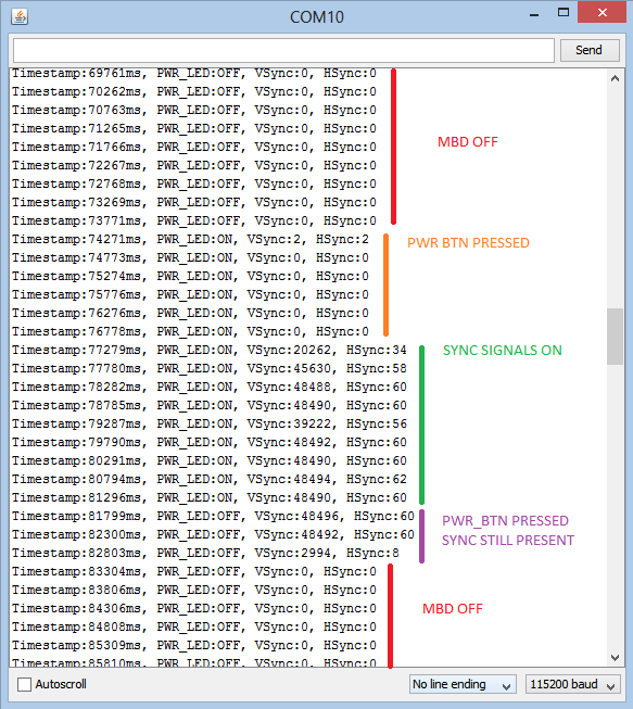
Here’s a proof of concept. The window shown above is Arduino serial monitor. I’ve connected the HSync and VSync pins to the interrupt pins of my Arduino, the PWR_LED output to an input pin and I ran the program. Initially you can see that the motherboard is off, because PWR_LED is off. I pressed the power button after the timestamp: 73771ms. PWR_LED turns on. The delay for the VSync and HSync signals to appear quantifies the delay (shown in orange) between PWR_BTN press event and video initialization. After timestamp 81296ms I pressed the PWR_BTN again and it turned off the video after a short delay which is exactly what I experience when I the monitor is connected. If you refer to the handy VGA timing calculator the 48.4kHz HSync and 60Hz VSync timing correspond to 1024×768 @ 60 Hz display mode which is exactly what I see on the monitor. The resolution also depends on the pixel clock so this may not be always accurate. Please ignore the instability of frequency readings because of wiggly connections.
Similar tests for DVI and HDMI.
Analog VGA will soon be deprecated and it is necessary to implement this on DVI and HDMI as well. DVI and HDMI are similar and electrically compatible. HDMI is more advanced and has some extras like 1) HDCP support for content protection, 2) LPCM audio stream, 3) CEC – Consumer Electronics Control commands. There are passive HDMI to DVI adapters for connecting HDMI cable to a DVI port. This means that designing the tests alone for DVI should take care of HDMI as well.
DVI connectors have three variations: DVI-A, DVI-D and DVI-I. DVI-A carries analog video signals similar Analog VGA. DVI-D carries video in 4 Transition Minimized Differential Signaling (TMDS) channels. DVI-D Dual-link is another variation of DVI-D that carries 8 TMDS channels to support even higher resolutions. TMDS, as Wikipedia defines it, is a technology for transmitting high-speed serial data and is used by the DVI and HDMI video interfaces. The transmitter incorporates coding algorithms which reduces EMI over copper cables and enables robust clock recovery at receiver to achieve high skew tolerance for driving longer cables as well as shorter low-cost cables. The physical layer of TMDS is Current-Mode-Logic (CML) which is similar to ECL but has positive polarity with the lower voltage swings of up to 400mV. This enables high speed communication while reducing the power consumption for portable devices.
I have gone through the DVI 1.0 and HDMI v1.3 specifications and I found the following clause in the DVI 1.0 specification as a life saver.
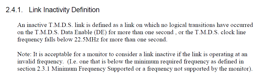
So this means I need to measure only the TMDS clock. The frequency of TMDS clock goes up to 165Mhz and Arduinos are not capable of measuring this much. So there will be a prescaler to divide the clock frequency.
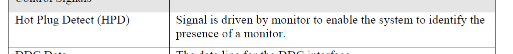
There’s also a Hot Plug pin that I need to pull up using an 800 ohm resistance. The pin is defined by the DVI spec as follows:
The Display ID Data EDID of the connected display is made available to the OS through the DDC/DDC2 link (I2C) in VGA as well as DVI and HDMI ports. The OS uses this data to get the ID and capabilities of the connected display. I’m assuming that EDID is not checked during boot up and a safe default display mode like VGA is used. The following blog post supports my assumption: http://blog.komeil.com/2008/06/fixing-edid-dvi-monitors-no-signal.html. The title suggests that it’s the operating system which has problems when EDID is missing.
So I have designed the circuit which appears correct to me as of now. It will need some testing when the parts arrive to see if it works.
KiCad schematic
I have made a preliminary schematic in EESchema for the test-interface board. Please take a look at it and let me know if you have concerns or suggestion.
There’s also one very important thing that I need to mention. After I finished making this schematic the ERC and netlisting were not working. EESchema crashed and threw an exception error. I spent half a day to figure out what’s so unusual about my design. It crashed on Ubuntu as well. So I deleted top half of the schematic to see if the error persists. It was still there. So I clicked undo and deleted the other half, it was fixed. Then I proceeded further with this bisection method and finally I found that using rectangular bracket [] in Hierarchical labels of the Display detector block was causing the problems. So if you’re a KiCad EDA user and here are the two things that I’d like to share:
- Use bisection search method to hunt down cause of unhandled exceptions.
- Never use rectangular brackets.
Did you report the bracket problem upstream? If not, why not?
Re. the 16-pin socket: you probably want to connect some other pins too. Especially pin 3 is often used for #reset. How about a block of 3-pin jumpers to select pull-down, pull-up or open connection for those pins?
Yes, I have reported the bracket problem on 8 Aug. You can see the updates here :
https://bugs.launchpad.net/kicad/+bug/1209424
For P7, the 16 pin DIP socket, I have referred to this pinout:
http://www.totalphase.com/image/docs/flash_socket_datasheet/soic16-pinout.png
Pin three is marked NC. To double check, I have referred to the datasheet of a random soic16 flash like http://www.farnell.com/datasheets/40260.pdf
Are there some specific type of SO-16 flash chips that I didn’t consider? If so, please send a datasheet.
Thanks,
Ayush