
Apologies for the late update. The design that I posted in the last post was more challenging than I had thought. However I’m happy to announce that my test hardware that I call ‘coreboot test interface board’ (TIB) is now complete. Only some of the software interface part is remaining in the project. So let me share with you a very quick update of last month. Continue reading GSoC (coreboot): Test interface board complete
Author: Ayush Sagar
GSoC (coreboot): Week 5-7 – Redesigning the test-interface-board
In the last blog post I talked about the test-interface-board. There were some concerns about the use of FT232H chip and extra features like voltage and temperature measurement were not required. Keeping in view all the suggestions and improving things on my side I have redesigned the board.
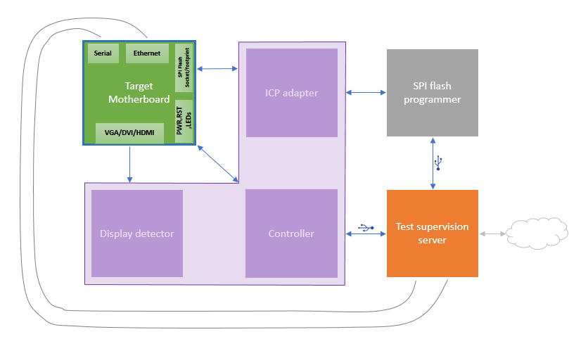
The figure above shows only one target board connected to the test supervision for simplicity. The purple L-block is the test-interface-board. This time, instead of using an integrated flasher I wish to support all existing flashers so I have developed an ICP adapter. An In-Circuit Programming (ICP) adapter contains the firmware flash memory removed from the motherboard and it acts as an electronic change-over switch that connects this flash memory to the motherboard or the programmer as required. It also includes logic-level translation to support as many as possible combinations of programmers and motherboards. The support for programmer voltage is in range 1.2V-5.5V and for motherboard SPI voltage it’s in range 1.65V-3.3V.
As a quick test for VGA initialization I’ve added video detection for Analog video (VGA), DVI and HDMI ports. This checks presence of signals that are only there when video is active. In other words, it checks whether a monitor’s status led would turn green if it’s plugged to the motherboard without actually plugging one. I have prepared schematics, some parts of which are yet to be validated through prototyping. This will all be implemented as an Arduino add-on board (aka Shield) for convenience and the Arduino would act as the controller.
The Serial and Ethernet ports can be connected in the usual way using Serial-to-USB cables, Ethernet cables and hubs. Continue reading GSoC (coreboot): Week 5-7 – Redesigning the test-interface-board
GSoC (coreboot): Week 3 and 4
In the past two weeks I was on vacation and I have been working on what I call “test interface board”. Before I go on to elaborate this I feel there’s a need to discuss the big picture of this project because a lot of things have changed for good reasons and the old terminologies don’t make sense.
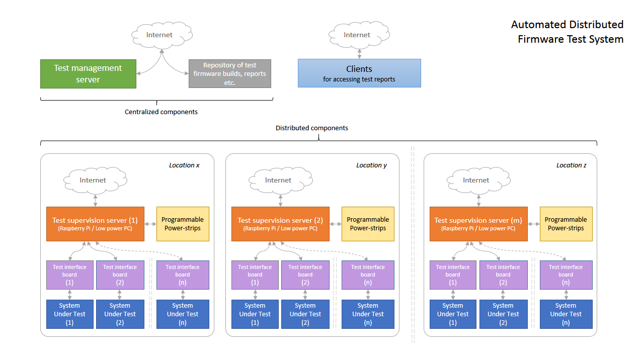
Just to remind, my project is centered on building inexpensive and flexible test-rig for the Automated Distributed Firmware Test System described in Quality Assurance Talk by Stefan Reinauer.
A centralized Test Management Server generates test sequences for remotely located systems under test (SUTs) and this includes controlling and monitoring the SUTs and flashing different firmware builds on them. The test management server coordinates with a repository for accessing test builds and for storing test reports. Test reports are the final and useful output of the whole system and these may be accessed using browser by clients from internet.
A Test Supervision Server is a low power computer that acts as a local housekeeper of SUTs for a given physical location. It connects to the Test Management Server using SSH over internet and executes given test sequences by coordinating closely with the SUTs using a Test Interface Board. Programmable power-strips are provided to control power supply to the SUTs from Test Supervision Server.
My work will be confined to the distributed components for now. I have completed the programmable power-strip block. A future add-on to this block could be integrating active power & energy measurement of an SUT for energy efficiency benchmarking. If this is really desirable it could be done after I finish doing the other parts. Right now I’m working on the Test Interface Board.
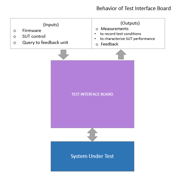
The Test Interface Board provides necessary hardware interface for connecting Test Supervision Server to an SUT. This is necessary to flash firmware to the ROM, to control power/reset sw, to measure PSU voltages and surface temp. of ICs and to take POST feedback if available. Let’s dive into more details to see how this can be done.
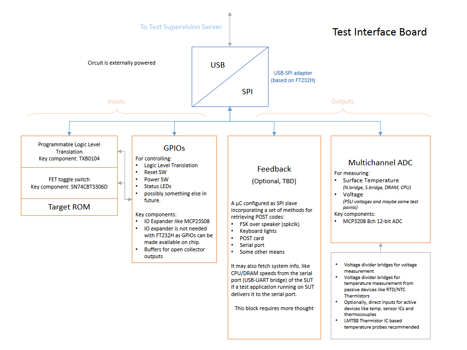
FT232H has a multipurpose serial engine that can be configured as SPI master. FT232H has additional pins that may be used as GPIOs so a GPIO expander may not be needed. The FT232H datasheet states that it offers up to 30mpbs throughput in synchronous serial mode which makes it a fast flashing solution for the given price point (3$). Slave Select (SS) pins can be used to switch between other devices like an ADC that gives voltage and temperature measurements and an optional Feedback microcontroller configured as an SPI slave that gives more information about the SUT. A few GPIO pins can be used to configure Logic Level Translator to ensure compatibility with serial flash of different voltages ranging from 1.8 V to 5V and a GPIO pin will also be used to configure a FET toggle switch (MUX) to electrically detach the serial flash for programming and connecting it back to the motherboard when it’s done.
Notice that I’ve got rid of microcontroller this time. This is because a new microcontroller chip doesn’t necessarily have a bootloader and it needs to be programmed using a dedicated programmer. This adds considerable cost and inconvenience for someone who needs to build only few of these boards. So unless you’re using the optional Feedback module nothing needs to be programmed. Just ordering the board and components and soldering up everything using a 15W iron should be enough to make one of these.
I’m also going to ensure modularity by having small PCBs for each functionality connected to a main-board using headers so that they can be developed independently and used as required. Also, there’s flexibility of choosing temperature probes because it is possible that someone already has good quality probes (that come with professional DMMs).
And a few comments about the ADC I’ve chosen – The ideal choice of ADC for voltage and temperature measurements where the sampling period is large is an integrating ADC. An integrating ADC charges a capacitor from the input signal for a known period of time using an opamp integrator then it discharges that capacitor using a known negative reference voltage. The time it takes to discharge the capacitor is proportional to average value (area under curve) of input signal over sampling period. It’s theoretically simple but it needs use of precision external components and a microcontroller program to work. This is the technique used in professional DMMs (True-RMS) and bench power supplies (for feedback). Delta-Sigma ADCs are common and cheap these days but they don’t average the values over time like integrating ADCs. However, they can provide acceptable accuracy for our application and MCP3208 is a good candidate.
Please see the figure for more details and let me know if there are concerns or suggestions. I’ll post more stuff and schematics in a couple of days.
GSoC (coreboot) Progress till week 2
As you might know my GSoC project is about making a test rig that can make coreboot test systems more accessible to a coreboot test server. This test rig enables coreboot test server to interact with the systems under test (which may be remotely located) in the following ways:
- Power supply control (discussed in this post)
- power/reset switch control, voltage and temperature readouts, firmware flashing on serial flash (to be done next)
- provision for POST feedback (later)
With this project I’m hoping to create an environment where developers will be able to conveniently connect their systems to the coreboot test server for testing at their own place. This is why I like to call it a distributed test environment as it facilitates mass testing without the need to maintain a dedicated testing facility.
So this week I will present a nice and easy solution for power control of the coreboot test systems. I would call this device a ‘programmable power strip’. Before going to the final solution let me first walk you through all the routes that I’ve taken in order to answer some potential questions that may arise. Read on…
Hello :)
I’m Ayush Sagar from India and I will be working with coreboot this summer on the project “Test set-up for the coreboot distributed firmware test environment featuring greater extensibility, enhanced automation, concurrent high speed firmware flashing and decentralized operation“ under Google Summer of Code 2013.
I’ve almost completed my graduation in Electrical & Electronics Engineering and by training I’m skilled at developing SCADA applications and ladder logic programs which are used for power system and factory automation. However my interests are widely scattered around physics, electrical engineering and computer science. I have been repairing consumer electronics and computer hardware on component level since a very long time as an earning hobby. It’s quite profitable here even today as most people are reluctant about throwing away their belongings. I’m also passionate about programming but I’m new to free and open source software development.