In the past two weeks I was on vacation and I have been working on what I call “test interface board”. Before I go on to elaborate this I feel there’s a need to discuss the big picture of this project because a lot of things have changed for good reasons and the old terminologies don’t make sense.
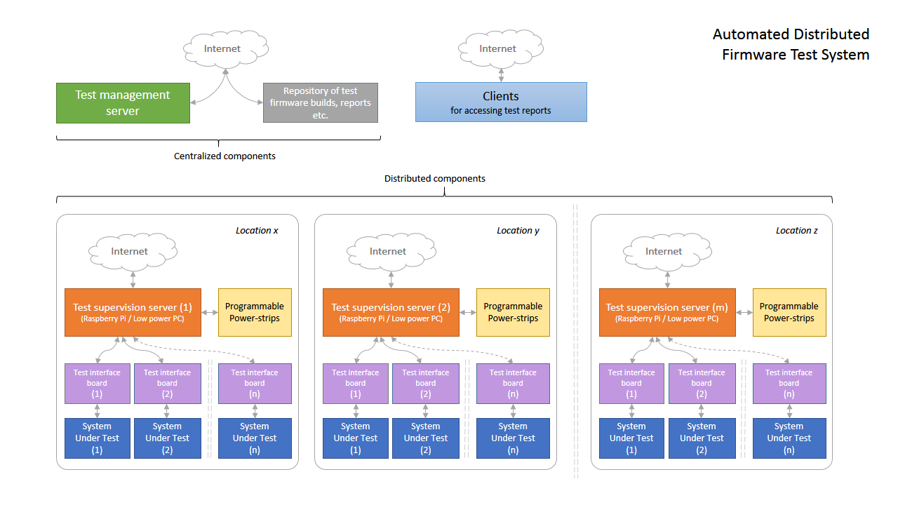
Just to remind, my project is centered on building inexpensive and flexible test-rig for the Automated Distributed Firmware Test System described in Quality Assurance Talk by Stefan Reinauer.
A centralized Test Management Server generates test sequences for remotely located systems under test (SUTs) and this includes controlling and monitoring the SUTs and flashing different firmware builds on them. The test management server coordinates with a repository for accessing test builds and for storing test reports. Test reports are the final and useful output of the whole system and these may be accessed using browser by clients from internet.
A Test Supervision Server is a low power computer that acts as a local housekeeper of SUTs for a given physical location. It connects to the Test Management Server using SSH over internet and executes given test sequences by coordinating closely with the SUTs using a Test Interface Board. Programmable power-strips are provided to control power supply to the SUTs from Test Supervision Server.
My work will be confined to the distributed components for now. I have completed the programmable power-strip block. A future add-on to this block could be integrating active power & energy measurement of an SUT for energy efficiency benchmarking. If this is really desirable it could be done after I finish doing the other parts. Right now I’m working on the Test Interface Board.
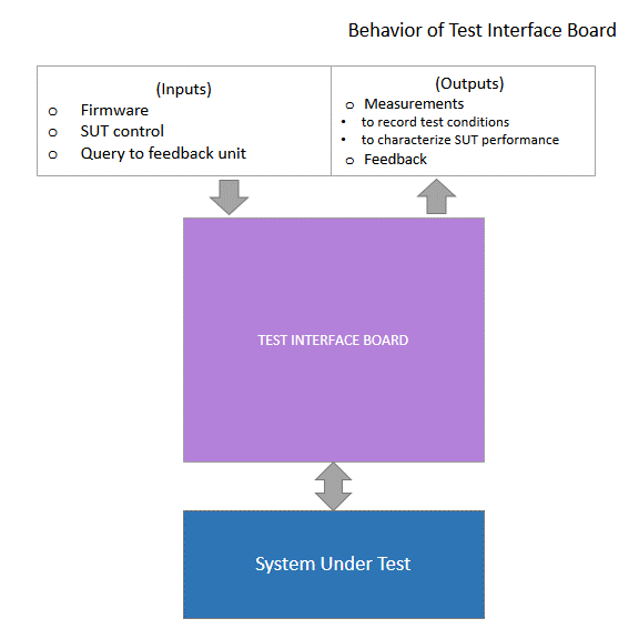
The Test Interface Board provides necessary hardware interface for connecting Test Supervision Server to an SUT. This is necessary to flash firmware to the ROM, to control power/reset sw, to measure PSU voltages and surface temp. of ICs and to take POST feedback if available. Let’s dive into more details to see how this can be done.
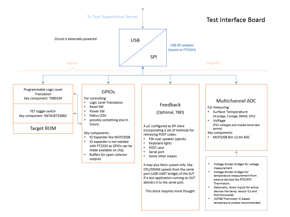
FT232H has a multipurpose serial engine that can be configured as SPI master. FT232H has additional pins that may be used as GPIOs so a GPIO expander may not be needed. The FT232H datasheet states that it offers up to 30mpbs throughput in synchronous serial mode which makes it a fast flashing solution for the given price point (3$). Slave Select (SS) pins can be used to switch between other devices like an ADC that gives voltage and temperature measurements and an optional Feedback microcontroller configured as an SPI slave that gives more information about the SUT. A few GPIO pins can be used to configure Logic Level Translator to ensure compatibility with serial flash of different voltages ranging from 1.8 V to 5V and a GPIO pin will also be used to configure a FET toggle switch (MUX) to electrically detach the serial flash for programming and connecting it back to the motherboard when it’s done.
Notice that I’ve got rid of microcontroller this time. This is because a new microcontroller chip doesn’t necessarily have a bootloader and it needs to be programmed using a dedicated programmer. This adds considerable cost and inconvenience for someone who needs to build only few of these boards. So unless you’re using the optional Feedback module nothing needs to be programmed. Just ordering the board and components and soldering up everything using a 15W iron should be enough to make one of these.
I’m also going to ensure modularity by having small PCBs for each functionality connected to a main-board using headers so that they can be developed independently and used as required. Also, there’s flexibility of choosing temperature probes because it is possible that someone already has good quality probes (that come with professional DMMs).
And a few comments about the ADC I’ve chosen – The ideal choice of ADC for voltage and temperature measurements where the sampling period is large is an integrating ADC. An integrating ADC charges a capacitor from the input signal for a known period of time using an opamp integrator then it discharges that capacitor using a known negative reference voltage. The time it takes to discharge the capacitor is proportional to average value (area under curve) of input signal over sampling period. It’s theoretically simple but it needs use of precision external components and a microcontroller program to work. This is the technique used in professional DMMs (True-RMS) and bench power supplies (for feedback). Delta-Sigma ADCs are common and cheap these days but they don’t average the values over time like integrating ADCs. However, they can provide acceptable accuracy for our application and MCP3208 is a good candidate.
Please see the figure for more details and let me know if there are concerns or suggestions. I’ll post more stuff and schematics in a couple of days.


