
Apologies for the late update. The design that I posted in the last post was more challenging than I had thought. However I’m happy to announce that my test hardware that I call ‘coreboot test interface board’ (TIB) is now complete. Only some of the software interface part is remaining in the project. So let me share with you a very quick update of last month.
After I posted the last update I started looking for the components. I chose SMD components that are easy to hand solder. Too small components are difficult to work with and big through-hole components take up board space and can add noise to the system. The chosen components are inexpensive, well-stocked, and come from reputable manufacturers. A bill-of materials is shared later in this post.
I had some discussion with Dave about this design and these things happened:
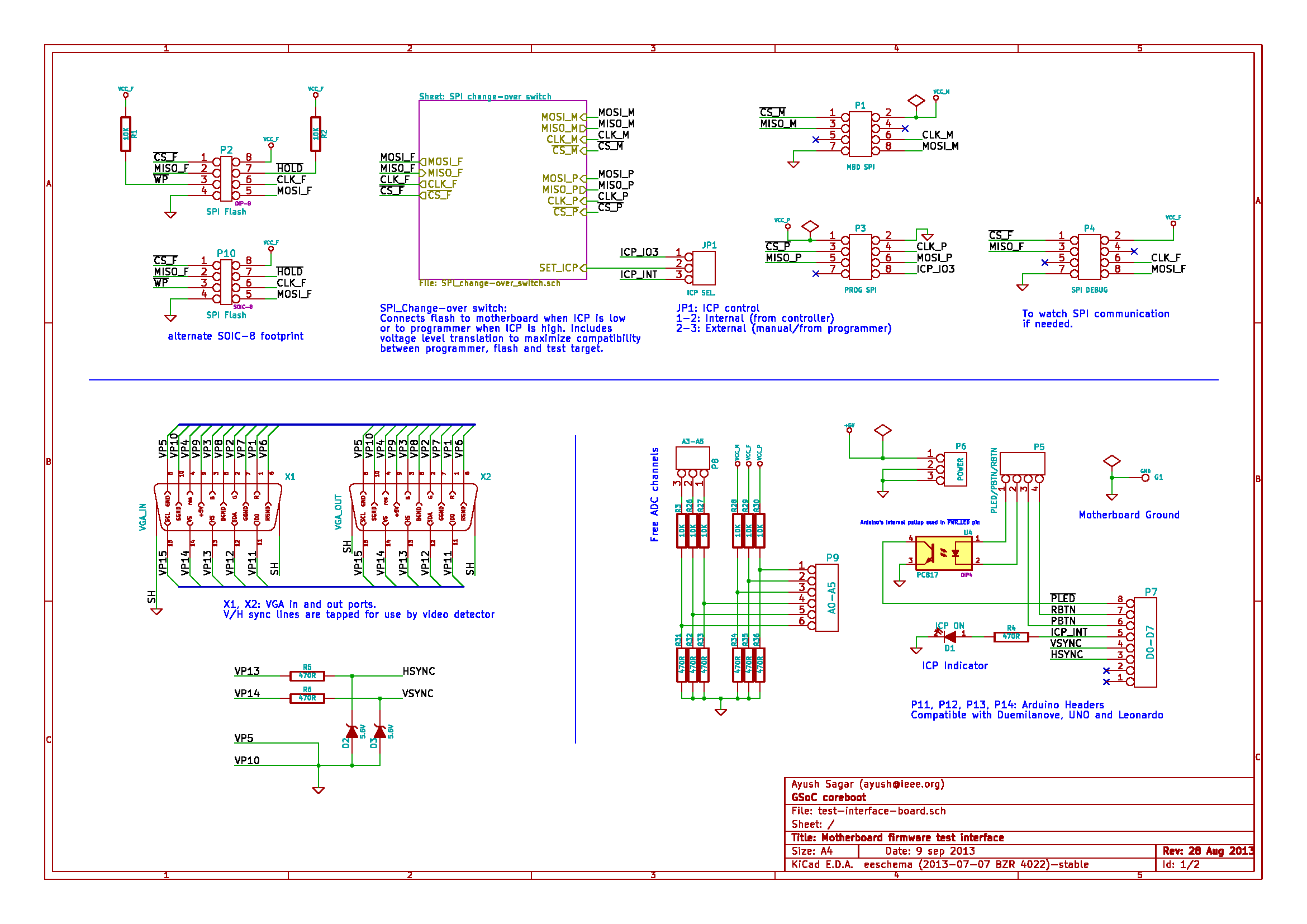
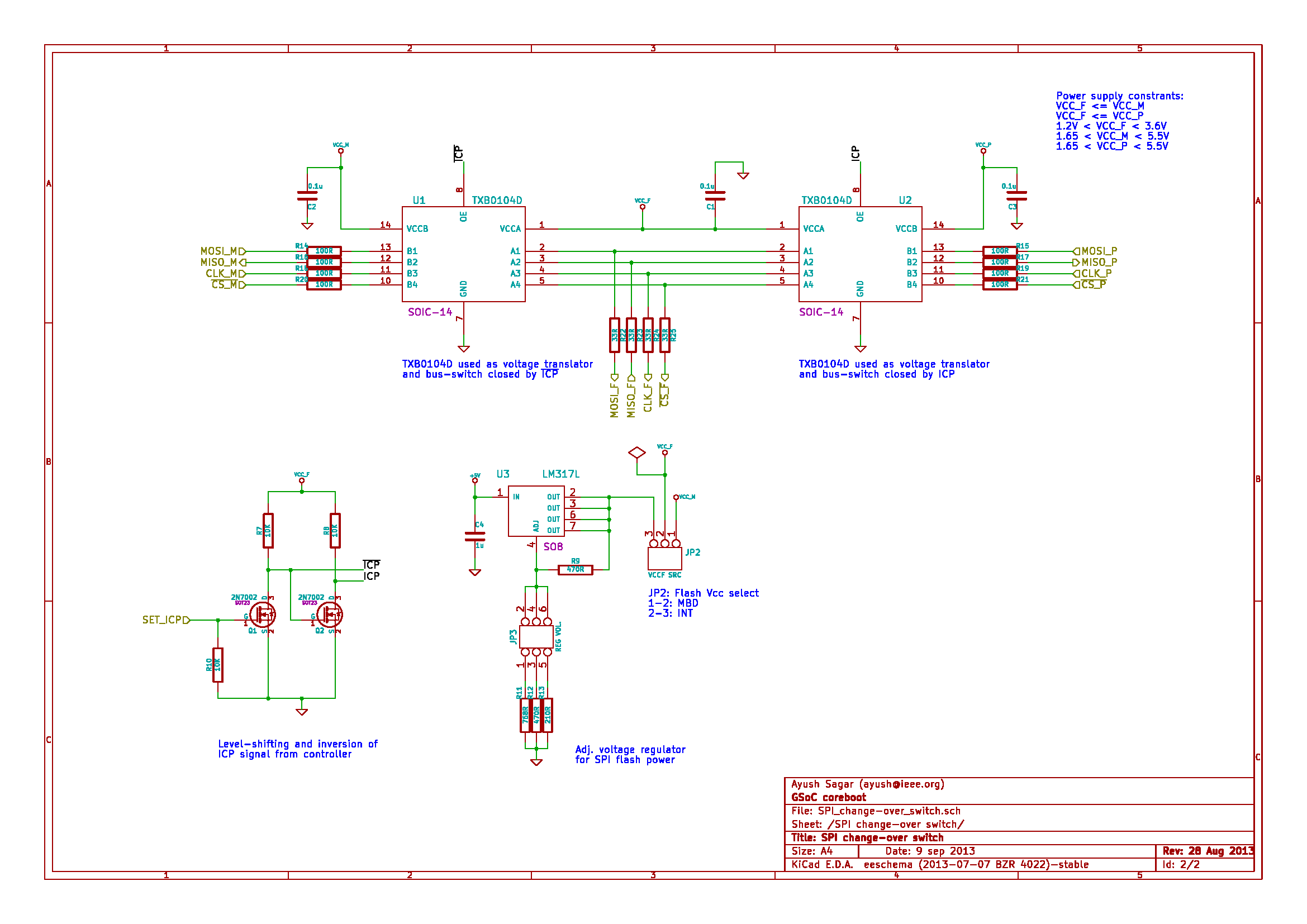
- We both found that the power supply design, i.e. the interaction of VCCF, VCCM and VCCP has some scope for improvement. So I replaced the bilateral analog switch with another TXB0104 translator. Logic levels of the three systems are now isolated.
- There’s a choice of choosing flash power source. It can be powered by the internal voltage regulator or motherboard. Choosing motherboard VCC can help to boot the board without powering on the TIB.
- Pot. was replaced by jumper presets of 1.8V, 2.5V and 3.3V. Pot based regulator was required in the earlier version as it needed close voltage matching between VCCM and VCCF in some cases.
- Added a SOIC8 footprint.
- Changed pin-outs for all SPI ports. Programmer side port pin-out is Dediprog compatible, motherboard side pin-out resembles the DIP8/SO8 flash chip pin-out for easy connection.
- Removed DIP-16 footprint. It takes board space and the stray tracks could potentially distort SPI signals. Instead of using 16 pin flash users can add a compatible DIP-8 flash to the parts list when ordering parts for building the TIB. In many cases they can keep their stock flash chip safe and unmodified.
- Removed inbuilt DVI/HDMI video detection circuit because cheap DVI to Analog VGA converters are available to buy for around $7 on eBay. It can be used with Analog VGA sync detection in this circuit. Having gone through so many documents and component datasheets related to DVI/HDMI related chips it’s really silly of me not to look for a converter on ebay. I saw the converter as an ad on some website, probably because of my google search history was related to DVI digital to analog conversion. This is the first time I felt personalized ads to be useful. Moreover, the CML-TTL converter chip (mc100ept21) I used in my schematic is 7 USD per piece on Mouser electronics. Although I had ordered those parts before I came to know about cheap converters I don’t see any point in developing this portion further.
So here’s the final schematic:
I had received the parts on 16th Aug that I had ordered from Mouser electronics. I was out of station for a week and I began prototyping after I had returned on 24th.
Prototyping and testing:
- I have a FT232H development board (UM232H) that I use as a programmer. It has a 30Mhz SPI clock.
- I ‘had’ an Asrock E350M1 board. I configured and built a coreboot image for it under Ubuntu 13.04. I chose to build with the default seabios payload and used the VGA bios as an option rom that was available to download on coreboot.org’s page on E350M1.
- Flashed it successfully to the Winbond W25Q32BV 4MB flash on the motherboard
- Now I have a test firmware image. Although this system can be tested on the stock firmware, I was really curious to see how fast coreboot is. I’m impressed! It boots faster that the time it takes for the monitor to set video on. And I can confirm that my Windows 8 installation worked fine on E350M1 with coreboot v4+seabios.
- I built a prototype for the SPI portion on breadboard.
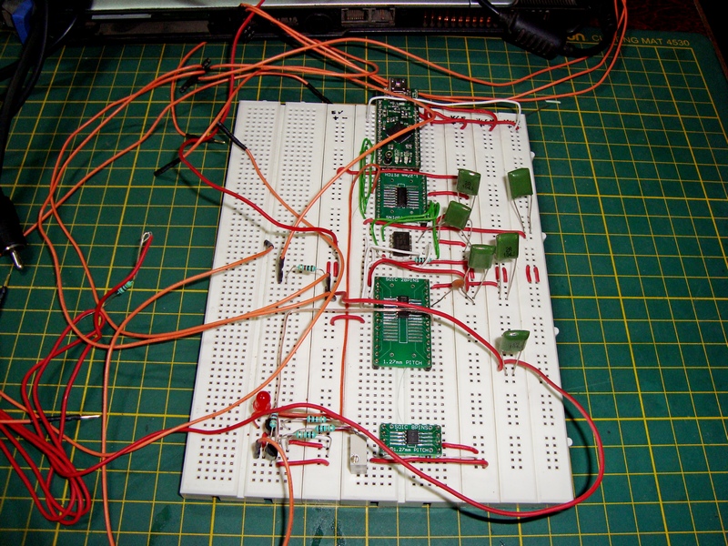
- Flashrom was not able to detect the flash chip. It seemed like the TXB0104 chips were not working at all.
- I tried shortest possible wires, tried different chips (I had ordered 4 pcs) to rule out defects but nothing really worked.
- The propagation delay was 3-5ns on the datasheets and that shouldn’t cause problems.
- May be the translator chip wasn’t getting enough drive? No, the output ports on FT232H can source 1ma as well as 8ma and also support an option for lower slew rate. Tried all settings by reprogramming the EEPROM using FTProg.
- I could see some intermittent behavior however. On touching the clock wires on breadboard it was showing the Winbond chip as Generic flash with no supported operations.
- I bypassed the translator for the clock pin and it worked. It detected the flash and was able to read, write and verify. Apparently a problem with clock translation. Maybe the translator delayed the clock? Can’t be sure unless I see the waveform.
- I was reluctant to buy an oscilloscope for several days because I may have plans to go abroad for masters degree next year and I may not be able to take my tools along with me. For several days I was trying to get access to an oscilloscope from somewhere. The best offer was an invite to the IIT Delhi’s Digital Electronics lab by a friend, where I could test my stuff for few minutes, pretending to be a student there. This wasn’t comfortable to me.
- So finally, I bought my own. I have been looking at reviews of entry level scopes (stalking them o_o) from past few years. Rigol DS1052E was always top on my wish-list, priced nearly $350. It’s probably the best value for money scope out there. This is 50Mhz 1GSa/s model but it can easily be upgraded to 100MHz model with a firmware hack. The 50Mhz limitation is within the firmware. It has been performing great and I love it. The reason that they limit this in firmware is that the analog front end needs more effort to calibrate and test for 100 MHz operation (as told by my dealer). However I’m more interested in qualitative data than quantitative, so it doesn’t matter to me.
- So after getting the scope I probed the clock line. I saw a waveform that looked like mountains. (Sorry, I was stressed up and I didn’t take pictures of many interesting things). They were wild and random voltage swings which had a span of -3 to +7V I guess. My programmer has logic level of +3.3V. This was nothing close to a square or sine wave. That’s a scary waveform! (Is it a fault with my programmer?) I disconnected the UM232H board from the breadboard and connected the probe directly on the pins. The waveform were nice and clean square-waves with some over/under shoot. It probably has a high-slew rate. Nothing to worry about.
- A funny thing happened. When I put the oscilloscope probe on CLK_P pin on the translator, flashrom worked. It detected the chip. I remove the probe it didn’t work. It shows it as a generic flash.
- The probe is usually modeled as a 20 pF, 10 Mohm RC circuit. So I connected 22pF ceramic capacitors on both CLK_P and CLK_F near the chip. Flashrom was now able to probe/read/write correctly. It appeared like the wires I use are picking up some noise and using an RF filter like PEMI4QFN from NXP could be a solution.
- Now I also tried connecting the motherboard SPI bus to my system. It didn’t work. Again, similar wild waveforms, needed a larger capacitor, 47pF.
- Then I wondered about the inductance of these jumper wires that I was using. Here’s a nice calculator: http://www.consultrsr.com/resources/eis/induct5.htm
- From this I estimated wire inductance to be nearly 150nH for my 1ft jumper wire.
- Figured out the impedance of the TXB0104 input ports from the datasheet. It is estimated to be around 20pF, when port B is working as input.
- Let’s do a simple model of the SPI clock line with this data and see how it behaves. Here’s a great online simulation tool.
- http://www.partsim.com/simulator/#12950
- I insist that you try this and see for yourself. On opening the link you’d a RLC circuit that represents a simple RLC model of this. The source is a clock pulse source, tuned to 16Mhz. That’s the speed of SPI clock on Asrock E350M1. Click on the ‘Play’ button and see the waveforms.
- Notice that I chose a resistance of 0.1 ohms to model the wires and their contact resistance. Now change it to 100 ohms and run simulation again. See the change!!
- 100 ohm Resistor apparently solves the problem. It wasn’t obvious at first to use a resistor as a simple solution to this, I had to revisit the basics of first-order circuits. The TXB0104 has complex behavior and different input impedance under different states. Having an oscilloscope, I experimentally determined 100 ohm to be the best value. Going higher than that reduces the bandwidth as it increases the time constant of the circuit. It required lot of patience and time to reach to this simple solution of putting 100 ohm resistors in series. Now I know why I see those resistor arrays on DRAM modules.
- Mrnuke, you should try adding resistors to the outputs from the ARM chip in VultureProg. It might help you with speed issues that might be troubling you 😉 Also, PCB tracks in general have higher inductance than wires for a given length.
- A good thing I need to mention is that the translators are ESD protected up to 15kV so it has some resistance against ESD damage due to normal handling. ESD precautions still has to be taken however for the safety of motherboard and flash programmer.
- One day, while I was playing with my stuff, the E350M1 motherboard refused to boot. I re-flashed stock firmware and tried putting the flash back to its socket, but the board didn’t boot. On probing the MOSI line on the chip it appeared that the motherboard was not sending anything to the flash when I powered it on. I tested with DMM, the pin was shorted to ground for some reason. Could be a shorted varistor/TVS diode (this happens a lot in cell-phones due to ESD damage). I tried putting a 3.3V external source on the pin to clear the short. The short disappeared but it still didn’t work. I looked for any open resistors near the south-bridge, but it appeared the SPI bus comes directly from the south-bridge chip. It was apparently the CMOS output stage that was shorted to ground. So it’s gone…. The board was shipped from US so no hopes of getting it repaired under warranty here. The eBay dealer is not even replying to me. $150 vaporized!! !@$!@%## !!!
But no worries, I had completed all the tests to my satisfaction. The cause of damage is unknown to me but I expect the following causes:
- Floating earth of the LCD monitor. I was getting slight shock when I touched the VGA cable. Floating ground could have exposed the SPI pins to dangerous potential difference from my touch.
- ESD damage.
- The 22pf capacitors were loosely connected to the breadboard and this might have allowed those wild voltage swings, causing the damage.
Some takeaways from my bad experience:
- Most interconnects that we use in daily life like USB have protection against certain kinds of abuse and ESD built into them. But I can assure you that the SPI bus on motherboards is fully UNPROTECTED. Use great care when playing with it.
- Always consider the effect of wire inductance and impedance of the load being driven. If the effect is not in your favor it can probably damage your stuff due to high negative voltage spikes. I hope you saw the simulation that I shared above.
- Always make sure that you connect ground of all systems first. Other pins should not even be touched before equalizing ground potentials. Eliminate floating ground if possible by ensuring that the AC outlets are properly grounded and three pin power cables are being used.
- Take all ESD precautions. Always remember that YOU have the special powers to ‘un-heal’ your MOS based circuits by a single magical ‘touch’. ESD damage may shorten your device’s life and can cause failure at a later stage if not immediately.
Now that the schematic has been validated and everything works as expected, I’ve done the PCB layout for this. I estimate that my design would work reliably on 50MHz SPI clock (and maybe more) which is the highest SPI clock I’ve seen in ICH datasheets.
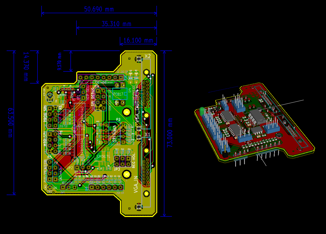
Here’s a pdf if you wish to see the silk screen on both sides properly:
The TIB is designed to fit on an Arduino as a shield. However, it can be used as a stand-alone device. That’s why I call it a board, not shield 😉
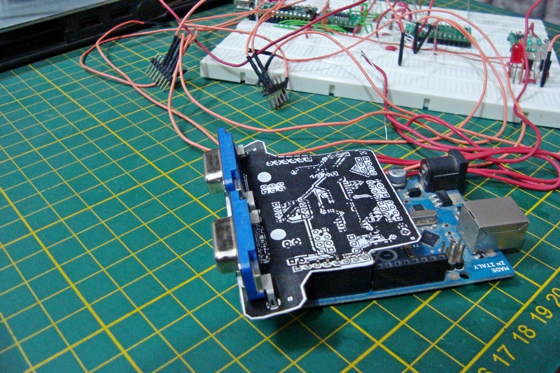
This is how it fits on an Arduino. There’s a cut in the PCB to make the unused digital pins accessible for any expansion in future. I’ve ordered my PCBs through seeedstudio.com. Thank you mrnuke for sharing your source 🙂 I should be able to get them in this week.
Here’s a bill-of-material for the components:
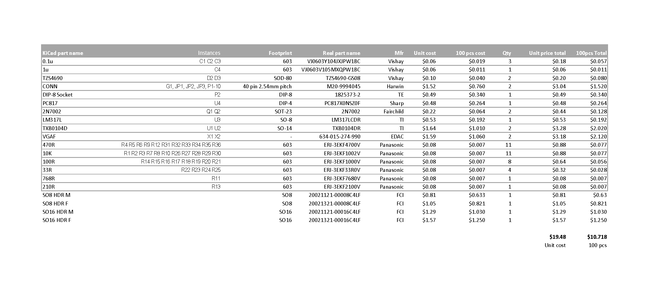
The prices are from Mouser electronics, dated 12 Aug 2013. These are the good quality components.
Use as a standalone device
A few words about the use of TIB without an Arduino: The SPI changeover switching, in-built flash, voltage translation are useful features. It provides a cheap and convenient method to test coreboot conveniently and safely for anyone who wants to work on coreboot for on their system. It saves the hassle of connecting test-clips every time.
I don’t recommend using test clips because the south-bridge SPI lines may not be at high-impedance state if the board hasn’t been turned off completely. Forcing signal into these lines can damage the south-bridge completely. There’s always some chance of shorting pins and making wrong connections when repeating this procedure. And people with laptops need to be more careful. Nobody replaces those high pin-count BGA chips like south-bridge and the entire motherboard needs to be replaced. Laptop motherboards are extremely expensive!
For stand-alone mode, irrelevant components can be ommitted, lowering the cost further.
Software part:
The Arduino firmware has been done. Works perfect. Here are the services that it provides:
- Query/set ICP mode if ICP jumper set to internal. Recall: ICP is a signal to connect the flash either to the motherboard or the programmer.
- Report whether VGA sync is present by measuring vertical and horizontal sync frequencies and checking whether it lies in the acceptable range. A frequency counter has been implemented using the hardware interrupts.
- Query power LED state to know whether the board has been successfully turned on/off.
- Operate Power and Reset buttons.
- Query VCCP, VCCF, VCCM to check for correct operation of the system. It uses statistical mode filter to filter out intermittent behavior of the ADC and the readings are referenced to the Atmega’s internal voltage reference instead of the power supply. So it gives accurate voltage reading reliably even with a single query.
- Query A3, A4, A5 voltages. They are extra ADC input for measuring any analog quantity. Optional.
To use, we send ASCII characters as commands over serial and it replies back for queries
Here are the commands:
- i Get ICP status. Replies ASCII ‘1’ if on ASCII ‘0’ if off
- I Toggle ICP
- v Get VGA sync presence. Replies ASCII ‘1’ if true ASCII ‘0’ if false
- f Get VGA sync frequencies. Replies (H,V) where H and V are sync frequencies in Hz.
- p Operate power switch for 500ms. Adding repeated characters would increase buttom press time. Say, if I need to turn off the board, I would send ‘pppppppp’ (8 times). This activates power button for 8*0.500 = 4s. Sending more characters adds time to the stop timer. So it ensures continuity of the button press when repeated characters are sent.
- r Operate reset switch for 500ms. Works in same way as above.
- l Get Power LED status. Replies ASCII ‘1’ if on ASCII ‘0’ if off
- P Get VCCP voltage
- F Get VCCF voltage
- M Get VCCM voltage
- 3 Get A3 voltage
- 4 Get A4 voltage
- 5 Get A5 voltage
Here’s the Arduino sketch: http://pastebin.com/aLVVyDL7
I’m trying to arrange another motherboard so that I can show you a video demo after I get the PCBs done. Coreboot supported boards are not easy to get here. That’s the reason I ordered E350M1 from US through eBay. The only board I’m getting here is ASUS F2A85-M. This is expensive, I’ll probably use just any board with SPI flash because my stuff doesn’t need coreboot at this stage to be tested.
So I’m happy to say that the hardware part of my project is complete. I’ve prepared a convenient hardware interface for setting up tests for coreboot on motherboard. The remaining work is to give convenient software interface to operate the test interface board, the USB power-strips and flashrom , all over SSH. The test server should also be able to uniquely identify the devices since more than one test targets may be connected to a local test management server test supervision server.
While I wait for the PCBs, I will be working on this software interface this week.
And once again, sorry for late and consolidated posts like this one. One of the reasons for this is that I have not been able to work in a logical order, where it would make sense of what I’m doing at each stage. Also, there were difficulties due to non-availability of stuff, expenses and transit times.