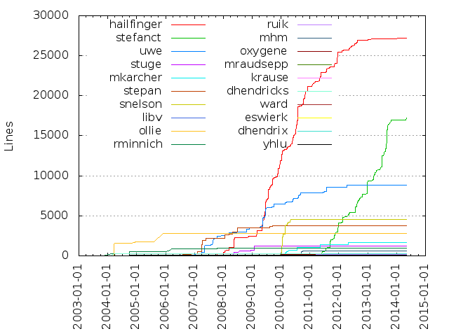
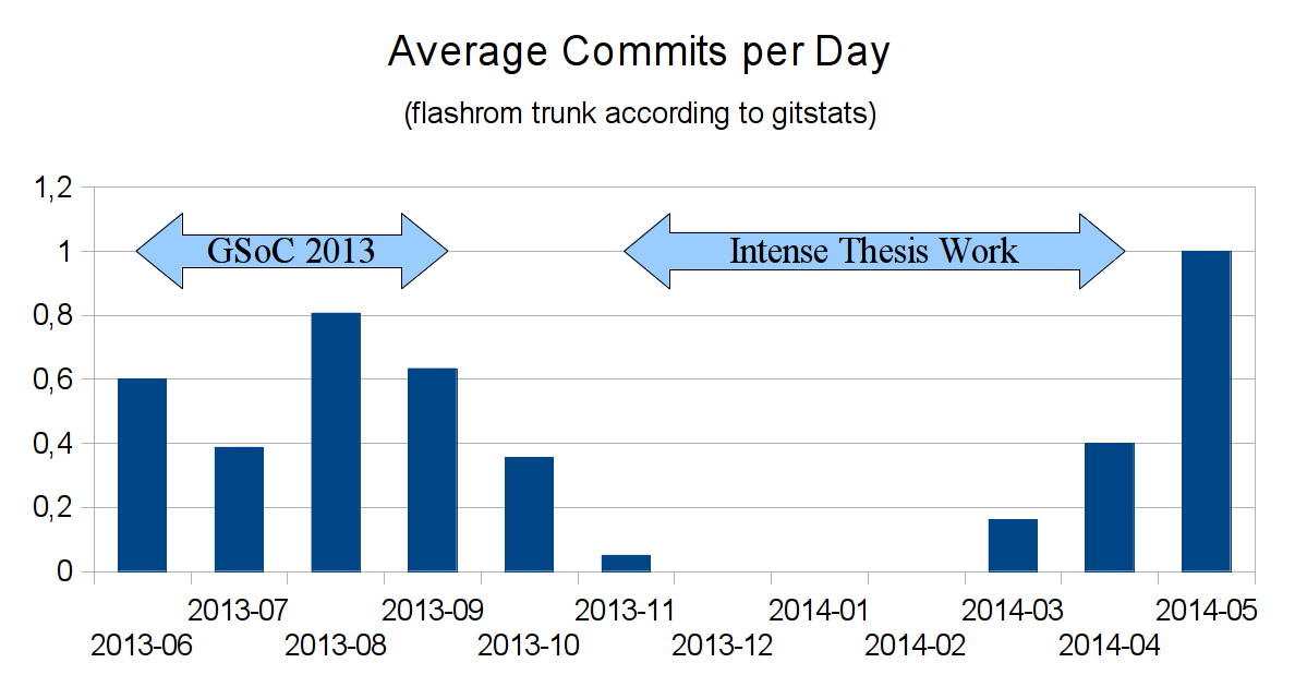
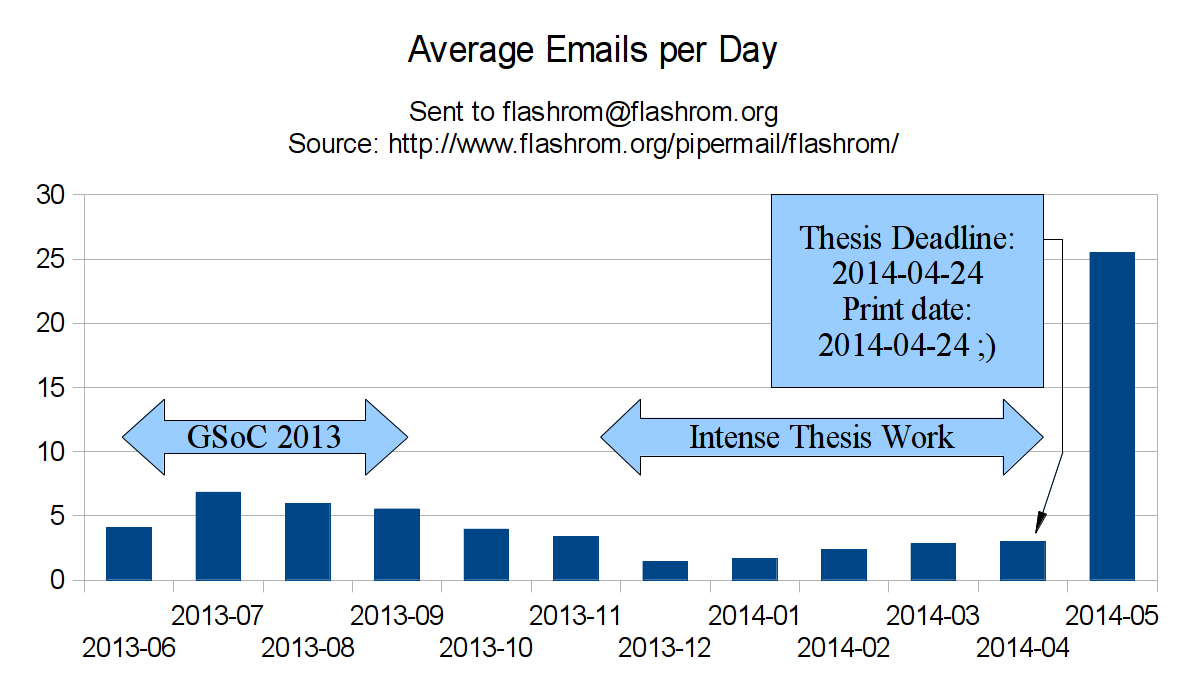
There is still no release, but we made quite some progress over the weekend. BSDs should work again as well as Windows (32b) – but the fix for 64b Windows will (most probably) not make it into 0.9.7 because we need to rework a bit of infrastructure code to get this right and we are not too sure about possible breakage from the quick hack I posted. We are still trying to verify the effectiveness of the IMC shutdown patch and looking for Dediprog testers with either an EM100 or a very old flash chip without fast reads. I expect the release to happen in the next two days. Now would be a good time to test flashrom’s trunk or my flashrom_0.9.7 branch on github on flash programmers near you. 😉
I would also welcome contributions to our brain storming about possible features of layout files. I decided to post them to the list instead of making a blog post out of it as envisioned in my last post.
DIY SOIC8 ZIF to DIP8 adapters
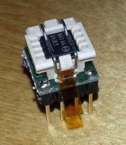
As mentioned previously I got an ASRock A180-H sample and want to develop Kabini support for flashrom with it. The board features an 8-pin DIP socket which is way easier to work with than a soldered flash chip, but the included DIP chip is the only one I possess. I do own quite a few SOIC chips though and 3 SOIC8 ZIF sockets though. And one of the two hacker spaces in town has these SOIC8 to DIP8 adapter PCBs in its inventory. So… of course I have built a SOIC8 ZIF to DIP8 adapter out of them.
Complete adapters are usually very expensive (>>50$) for no good reason (from a customer’s perspective only), so building such an adapter is the logical conclusion. Instead of the PCBs from futurlec mentioned above there is a very good deal available from adafruit. The cheapest SOIC ZIF sockets I could find are made by Wieson. They have 3 models available – for “200 mil” 8-pin (G6179-10), “209 mil” 8-pin (G6179-200000) and 16 pin (G6179-070000) chips. They are available from siliconkit (US, 2.5$ per 8-pin adapter, 10 pcs minimum), dediprog (Taiwan, 30$, 15 pcs package), and bios-repair.co.uk (UK, 5£) and probably elsewhere. I am using the G6179-10 below – IMHO the difference of the two 8-pin variants is the length of the chip to be inserted, not its width.
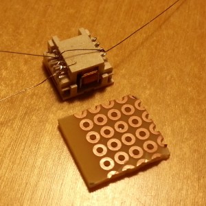
Before acquiring a pre-etched PCB I tried to solder a breakout board myself, similar to this tutorial:

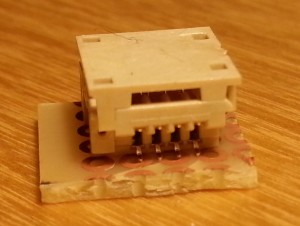
Attaching the wires works somewhat (but one needs steady hands and a lot of patience) but there is one major issue: there is just not enough space to fit the SOIC footprint inside the outline of the DIP pins (the DIP rows of the socket on the mainboard are 0.3″/~8mm apart, the SOIC chip including the pins is about the same size), and of course the pitch is so different that one can’t just solder it on top:

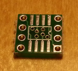
One could try solving this by rotating one of the footprints about 90° and routing the connections manually with enameled wires, but I very much prefer PCBs like this one:

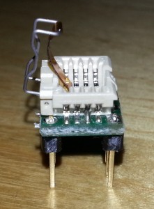
Here is the end result with the futurlec PCB which took me a fraction of the time I wrestled with the manual breakout approach:

All pictures above are taken by myself and put into public domain.

