Weeeeeee, we got the release out.
Category: flashrom
A brief progress sheet
Last week, I laid out a list of things to do in order to get more of the protocol finalized. Most of the items are crossed off, however, one little item remains standing. This item, while innocent and seemingly harmless is more painful than falling on your buttocks from a 10 story building on solid granite. Let’s have a look at why this small item is of such significance.
-
new API call set_chip_size()
When people think of QiProg, they think of one gadget with one flash chip connected. This is the common case, and, for the foreseeable future, will be the de-facto way of using QIProg. However, the original USB specification was intended for a broader use case: a programmer with several, individually addressable chips connected. One who observes the qiprog_read_chip_id() call will notice that it translates to a READ_CHIP_ID request over USB. This request will return identification data for up to nine chips. Aye, there’s the rub.
How does this play into set_chip_size()? Simple, set_chip_size for which chip? Do we send a flat list of nine uint32_t sizes, thus only needing one round-trip (control request) for all chips? Do we use the wIndex field of the round-trip, at the cost of needing one such trip for each chip? Once this question is answered, it will determine the answer for set_[erase/write]_[size/command] call and their respective USB round-trips, thus completing the USB protocol, and bringing QiProg to a usable state.
It’s easy to see why this one little detail is a blocker for all other remaining issues. I am leaning towards the use of wIndex (not the glass cleaner). Implementing a new control request in software and firmware is a matter of minutes. Testing it, and making sure it works properly is, at most, a two hour endeavor. Getting the design right: priceless.
Experiments of mind
The time for writing code is over. The time to design hardware is over. After seven weeks, the 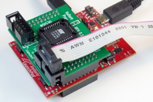 beginning has come to an abrupt end. I am severely behind schedule. In week seven I was supposed to implement erase functionality — tell the programmer how to erase the chip. This is not done. On the other hand, I have had code for weeks 8 and 9 almost ready, and just merged most of it last week. So, where am I? Am I ahead or behind schedule?
The fallacy of preemption
One of the requirements for applying as a GSoC coreboot student was to have a fully established, 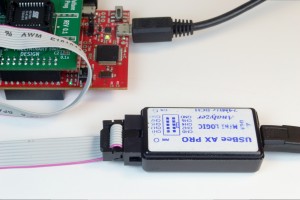 schedule from day[-1]. Establishing this schedule was a great experience, and it allowed me to think in depth about the problem and possible solutions — to a certain degree. I picked the steps I considered logical, in the order which I saw logical. Development is never about writing code in the order in which it will be executed. In this particular case, it was much easier to implement bulk writing without a predefined erase/write strategy, opting instead for a default just-do-it approach.
Why is this approach better than following the schedule, from a development point of view? We have had bulk read partially working for a while now. From the host point of view, reading and writing are symmetrical operations. The bulk of the code (pun definitely intended) is shared between the read and write operation. They both juggle data on the same endpoint. The only difference is the endpoint direction bit. It therefore made sense, once bulk reading was fixed for corner cases, to uses the same code to send data to the programmer. Making the programmer write that data was a matter of a couple of hours. There was no sensible reason to wait an additional two weeks before implementing this last bit.
Software development work is as much about making things work, as it is about the application of programming principles with unquestionable moral authority and correctness. In this case, implementing a trivial extension reusing code fresh in my mind was the preferred approach. Not only did it save me time by not having to re-examine the situation a few weeks from now, it also allows me to have a working program/verify scenario when implementing the erase strategies. As one might imagine, this makes the problem a lot easier. Attempting to preempt and enforce a schedule before the problem is thoroughly explored, occasionally conflicts with best practices of development. With this in mind, I am neither behind, nor ahead of schedule. I am precisely where I need to be.
A matter of experimentation
Most of the infrastructure and code is already in place. Bringing QiProg to completion is no longer an issue of adding functionality through code, but rather completing functionality by connecting the existing code. One issue I discovered after testing the bulk program code was a terrible race condition between read prefetching and the write loop. The prefetch logic incremented the internal address before data arrived. As a result, the new data would get written at the wrong address. Choosing the best solution to the problem is a matter of experimentation.
The “this won’t work because of that” and “what if this” turned into a series of exhausting thought experiments. I have been bugging Peter a lot in the past few days about a series of potential issues. Through tiring thought experimentation, we eventually agreed that the best way to proceed was to abstract a lot more through the API. This is a non-exhaustive list of the decisions we’ve made in the past week:
- set_address() is hidden from the API
- the internal address range is not exhausted once read or written
- read and write operations must not be interdependent, the internal read and write pointers will be distinct (as a side effect, this change also eliminates the race condition depicted above)
- set_address() + readn() turns into read(dev, where, n)
- All API addresses begin at 0. The programmer translates that into an absolute address
- new API call set_chip_size()
- new API call to explicitly erase blocks or sectors (to be defined)
- implicit erase on write can be enabled or disabled (to be defined)
- implicit erase will erase the sector/block right before the first byte of the sector is written
- exposing any USB specific dependencies in the API is strictly forbidden
My focus for the remainder of this week will be to shorten this list as much as possible. Once the dependency between read and write is unshackled, I will be able to erase/program/verify my faithful SST 49LF080A. From here, it will be a matter of finalizing and implementing the last obscure bits of the specification.
The state of QiProg for flashrom
As QiProg is still being finalized, implementing it as a flashrom programmer is still a long ways ahead. I do estimate that weeks 11 and 12 will provide ample time to integrate everything into flashrom, hopefully, in time for the 0.9.8 release.
GSoC 2013 [flashrom] blog post #5
The running gag that is not funny at all: new flashrom release will be out very soon! 😛
There are mainly two reasons why it was not released yet. First we have found a regression due to the inclusion of flash chips bigger than 16 MB and then I was working on adding decent support for a new SPI programmer before release. Continue reading GSoC 2013 [flashrom] blog post #5
VultureProg command center

It was time to upgrade. I got a new desk last week. For me, a piece of furniture is as boring as watching stainless steel rust (it does rust eventually). A desk, on the other hand, is anathema to replace. I have 20+ wires connected to my workstation going in all sorts of places. I like to keep these wires carefully routed and out of sight, a task made all the more difficult by the lack of any wire management gizmos on new desks. Consequently, after I get a new desk, you are well within your rights to imagine me grabbing my drilling machine, a set of saw cutter bits and an assortment of hole covers — and you need not wait long to see it. Needless to say, getting back up and running has taken a few days, but we are back with a shiny new VultureProg command center (pictured above for your viewing convenience).
The 80-20 rule
In 2011 I used to work developing Android apps. My boss told me “you will spend 20% of the time writing 80% of the code, and you will spend the remaining 80% of the time writing the remaining 20% of the code”. Sadly, QiProg has proven to not be an exception to this rule. Although I have consistently fixed issues and improved the layout of the code, the number of lines of code has been more or less stagnating after the first three weeks of exponential growth. I know how to erase the chip, I know how to program the chip, I know how to read the chip, and I have code to do all that. I just have not yet had the chance to hook it up to the ecosystem.
I am currently working on improving the bulk reading code. There are a few corner cases which are not well handled. As expected, it is taking a lot of time, and I even had to write a special testcase before I started.
Did you want fries with that?
Although we know how to handle every single aspect of the identify/read/erase/write/verify cycle, finding a way of connecting everything together in a simple, elegant, and efficient manner is a different story altogether. We have three API calls for handling erase and write, namely qiprog_set_erase_size, qiprog_set_erase_command, and qiprog_set_write_command. Peter wants everything to work without requiring an explicit erase. In his view, the VultureProg firmware should automatically erase a sector that is being written. Although this would simplify dumb cases where the whole chip or large sections of a chip are written at once, it spells disaster for flashrom’s aggressive optimization. What happens if the first part of a block matches contents, and flashrom decides to write the other part without needing an erase? VultureProg would erase the entire block, then write the second part to the block we never meant to erase. Questions such as this one need to be carefully thought over and elegantly answered. If I blindly start putting all the code together right now, I’ll most certainly have to fix it later.
Postal patronage
I received a very interesting package last week. I had a deal with Idwer to get him rid of a few LPC and FWH flash chips. I was able to take them off his hands for just a few euros, a deal made sweeter by the fact that those chips are no longer being sold anywhere. I also sent Peter a VultureProg board. Since he already has a Stellaris or two, I have just recruited an eager tester.
Can you send me a board?
Short answer, no. Just grab the gerbers and take them to SeeedStudio. They will be able to get boards in your hands for much less than what I pay to ship them. The two SMD capacitors are not hard to assemble. If you still want me to send you an assembled PCB, I will charge $50 (international) or $30 (US). I don’t have the physical time to sit and assemble PCBs by hand, plus, it would be very un-geekish of you to not assemble your own.
VultureProg: Equipped for galactic travel
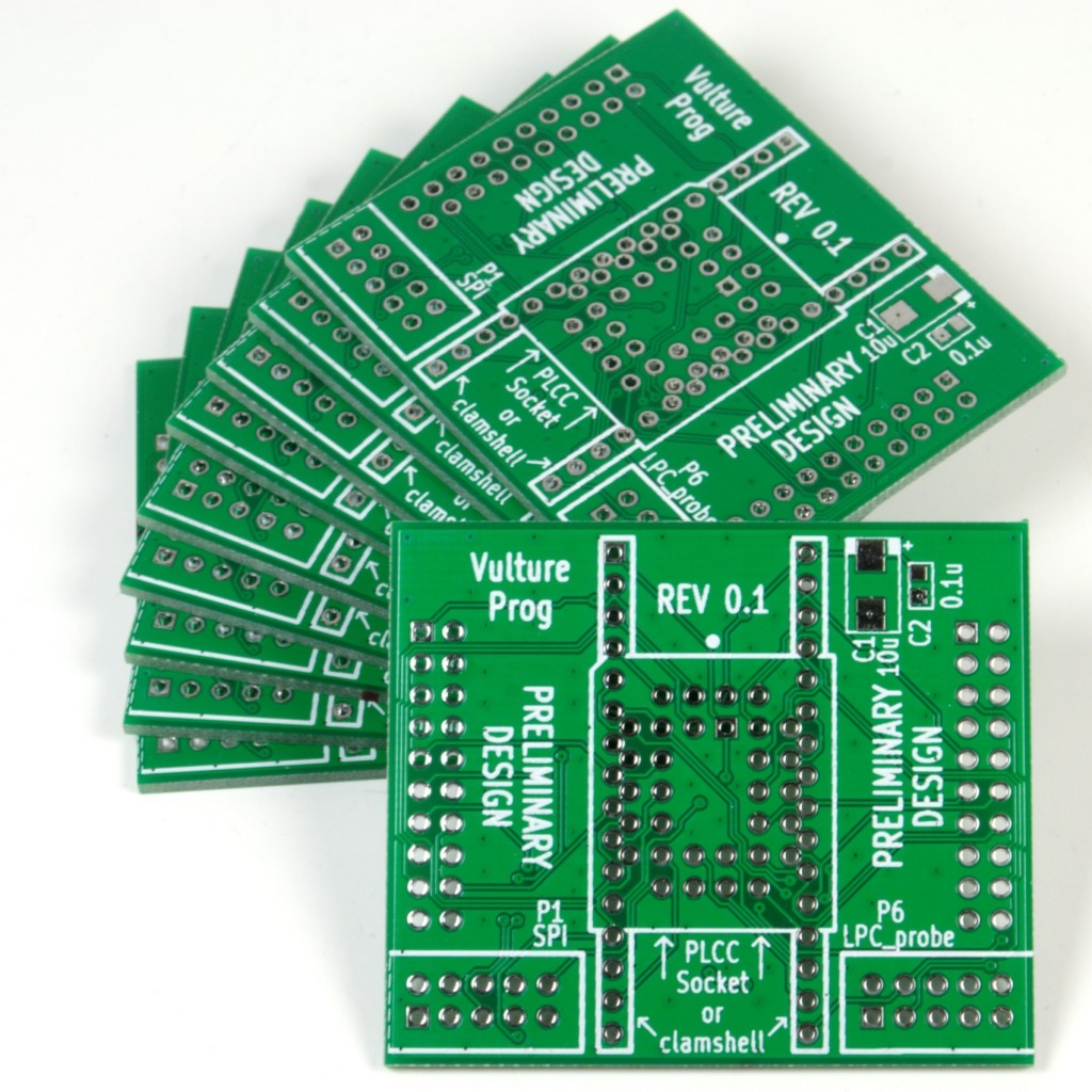
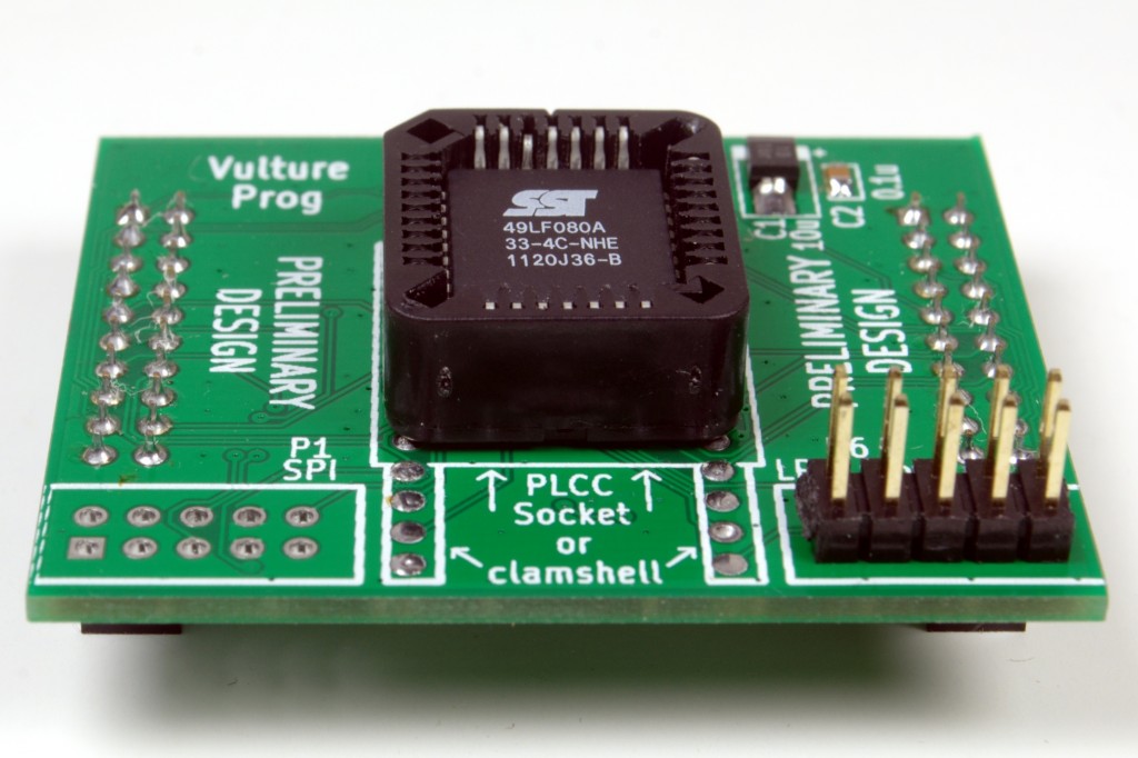
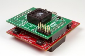 It’s here! And it’s ready for takeoff. The VultureProg PCBs have finally arrived, and it is time to turn VultureProg from a proof-of-concept toy to a serious galactic tool. My major concern was that I could have misrouted one or two connections. The LAD pins are particularly sensitive, as they need to be mapped to sequential GPIO pins, and start from GPIO0, otherwise we need to do bitshitfs in every LPC cycle, killing any hope of decent performance. I was also worried that the particularly tight tolerances could be problematic during manufacture. Everything works as expected. Enough words, let’s see the porn.
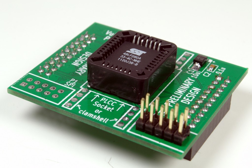
From bitstream to reality
I found it interesting to look at the transformation from a spaghetti on the screen to something real, something tangible.

No thorough and thoughtful post today. I have a new toy.
QiProg: Expanding the flight range
Today is disappointing. I was expecting to have gotten the first batch of VultureProg PCBs. Having  arrived in the US on Tuesday, I did not expect the package to be hovering in New York for most of this week. The need for eating the spaghetti and eliminating the hanging wires is growing more and more urgent with each speed increase. The long wires and insane inductance is already getting in the way of the signals, the lack of physical portability of the test setup is annoying, and the pain of accidentally knocking out a few wires is unbearable. Where are my PCBs ?!!!
High speed tests
The Stellaris is getting faster, much faster than initially predicted. From the pathetic 23 KiB/s read speed during the first tests, it now comfortably does over 450 KiB/s. The emulated LPC bus goes so fast, that I need to lower the CPU’s core clock down to a measly 16MHz to be able to just capture all the details of the waveforms.
Too much impedance
24MHz logic analyzer + Nyquist theorem = 12+MHz LPC clock
We’re pushing a 12MHz signal through 20+ centimeter hanging wires, routing them through a solder-less breadboard, then a socket, with the added load of probe wires. I was getting random errors or bad data, yet as soon as I disconnected the probe wires, everything magically worked. It must have had something to do with signal rise and fall times. On the Stellaris, this was relatively easy to cheat and fix by increasing the drive strength.
Where’s my bandwidth?
450 KiB/s * 1024 * 17 clocks/byte = 8 MHz LPC clock
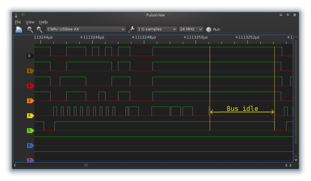
Something does not add up. We know we’re running at over 12MHz because we can not sample the signal well, yet the throughput is much smaller. The USB on the Stellaris is easily capable of 1 MiB/s. To quote Seconds from Disaster, “when investigators looked at […], what they found shocked them”:
The LPC bus is idle 30% of the time. We’re driving the bus so fast, that loop overhead is not only noticeable, but significant. Killing this overhead has the potential to bring the speed to 600 KiB/s.
Insect season
It’s a hot summer in Houston, with air conditioning running around the clock. Stepping in the hot, wet weather outside results in an instant cascade of sweat. Insects are crawling from every nick and crevice, fire ants are spawning from the underground in huge mounds, and mosquitoes are raising their own deadly army of high-pitched buzzers. The QiProg and VultureProg trees are no different.
I’ve made the executive decision to fix bugs as soon as they are getting in the way. I intentionally avoid the use of the term found. I can find my own damn bugs, however, it’s fixing them that is the problem. I prefer to have all the pieces in place before I polish and shine them.
A ripe testing ground
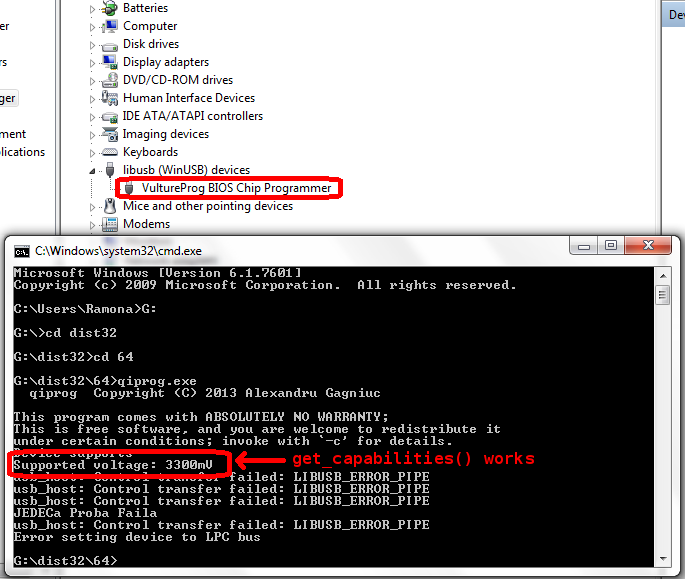
Out of curiosity, I wanted to see if VultureProg will work on Install’n’Pray operating systems (InP). InP are known for their excellent ability to expose even the smallest, most innocent problems, and expose problems where there are none. If VultureProg can work in an InP environment, it most certainly will be stable in unix-like environments. Although it did not work at first, testing on InP has lead to a number of fixes.
Where next?
We have bulk reading completed, which was initially scheduled for week 6. Weeks 7 and 8 look scary, with a lot of goodies, including program and erase functionality. I’ve decided to peek early into how to program and erase LPC chips. I found flashrom’s jedec.c to be of great help: QiProg knows how to byte-program and erase JEDEC-compliant chips. A lot is still scattered in topic branches here and there, waiting for one’s mercy to merge. Somebody please send me some coffee.
GSoC 2013 [flashrom] week #4
There is still no release, but we made quite some progress over the weekend. BSDs should work again as well as Windows (32b) – but the fix for 64b Windows will (most probably) not make it into 0.9.7 because we need to rework a bit of infrastructure code to get this right and we are not too sure about possible breakage from the quick hack I posted. We are still trying to verify the effectiveness of the IMC shutdown patch and looking for Dediprog testers with either an EM100 or a very old flash chip without fast reads. I expect the release to happen in the next two days. Now would be a good time to test flashrom’s trunk or my flashrom_0.9.7 branch on github on flash programmers near you. 😉
I would also welcome contributions to our brain storming about possible features of layout files. I decided to post them to the list instead of making a blog post out of it as envisioned in my last post.
DIY SOIC8 ZIF to DIP8 adapters
As mentioned previously I got an ASRock A180-H sample and want to develop Kabini support for flashrom with it. The board features an 8-pin DIP socket which is way easier to work with than a soldered flash chip, but the included DIP chip is the only one I possess. I do own quite a few SOIC chips though and 3 SOIC8 ZIF sockets though. And one of the two hacker spaces in town has these SOIC8 to DIP8 adapter PCBs in its inventory. So… of course I have built a SOIC8 ZIF to DIP8 adapter out of them.
Complete adapters are usually very expensive (>>50$) for no good reason (from a customer’s perspective only), so building such an adapter is the logical conclusion. Instead of the PCBs from futurlec mentioned above there is a very good deal available from adafruit. The cheapest SOIC ZIF sockets I could find are made by Wieson. They have 3 models available – for “200 mil” 8-pin (G6179-10), “209 mil” 8-pin (G6179-200000) and 16 pin (G6179-070000) chips. They are available from siliconkit (US, 2.5$ per 8-pin adapter, 10 pcs minimum), dediprog (Taiwan, 30$, 15 pcs package), and bios-repair.co.uk (UK, 5£) and probably elsewhere. I am using the G6179-10 below – IMHO the difference of the two 8-pin variants is the length of the chip to be inserted, not its width.
Before acquiring a pre-etched PCB I tried to solder a breakout board myself, similar to this tutorial:
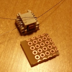
Attaching the wires works somewhat (but one needs steady hands and a lot of patience) but there is one major issue: there is just not enough space to fit the SOIC footprint inside the outline of the DIP pins (the DIP rows of the socket on the mainboard are 0.3″/~8mm apart, the SOIC chip including the pins is about the same size), and of course the pitch is so different that one can’t just solder it on top:
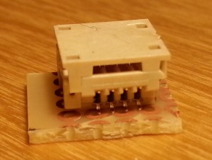
One could try solving this by rotating one of the footprints about 90° and routing the connections manually with enameled wires, but I very much prefer PCBs like this one:
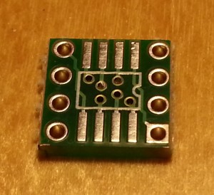
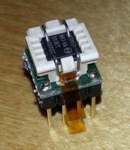
Here is the end result with the futurlec PCB which took me a fraction of the time I wrestled with the manual breakout approach: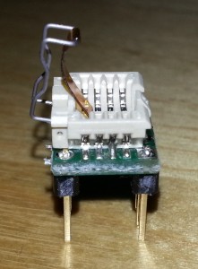
GSoC 2013 [flashrom] week #3
After enjoying an extended weekend at the customs office the Micron chips finally arrived at my place and I began testing them with flashrom while preparing parts of this post. One has quite a lot of idle time when testing bigger flash chips with a lousy self-made programmer… the execution of flashrom -w with random data took 52m58s on a 16MB chip (N25Q128) to complete (which is actually two complete reads and one complete erase + read + write cycle per block). Oh if only there would be a cheap but awesome open USB programmer… 😉
Carl-Daniel was still missing till I called him at work yesterday, so Continue reading GSoC 2013 [flashrom] week #3
Cooking with thin spaghetti: The hard side of Vultureprog
One of the reasons I fell in love with the Stellaris Launchpad boards is that they are modularly 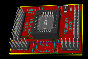 expandable. This notion is difficult to explain without comparison to STM Discovery boards, which have a row or two of pins on each side. The idea is simple: you hook one end of your wire to the right pin, and the other end to your breadboard, or you design a custom baseboard specific to the Discovery model. Stellaris takes this idea a little further. The layout of the pins is standardized, not just for the Stellaris, but across the family of TI development boards. Enter the Booster Packs: standardized add-on modules for TI boards. These modules are stackable, so it is possible to connect more than one to a single Stellaris board. This is why I wanted to use the Stellaris for this project. It’s much easier to build a booster pack than to tell people how to connect 32 wires; most people have problems connecting four of them to a buspirate. Let’s look at some of the design choices.
Constraints, constraints, constraints
It’s easy to imagine connecting a LPC chip: six wires and power. In reality, the situation is nowhere near as bright. Four ID pins need to be pulled low, reset pins (yes, there is more than one) need to be pulled high, and some pins simply cannot be left floating. Thus, even a simple bus like LPC becomes a nightmare. Without a logic analyzer to tell what works and what does not, the result is frustration and even self-inflicted injuries. Consequently, I wanted to do a few things right from the beginning(TM).
The most important point was to have all pins properly connected with zero wires. Users should not have to worry about what connects to where. Remember, these chips have 32 pins.
I also wanted to support all possible bus types. LPC and FWH are identical hardware-wise, and are not a problem to support concurrently. SPI is also just a few extra traces that lead to a header. On the other hand, having a programmer that also supports parallel mode is a much harder problem. It turns out there are really two “parallel” modes. The first one is ISA, where the chip is accessed via a linear address space. You put the address you want to access on the address pins, handle a couple of handshake lines to tell the chip if you want to read or write, and move the data over a separate 8-bit data bus.
On the other hand, the second “parallel” mode is a real pain. It uses a 2-dimensional address space, where you need to drive a row address, then a column address, and only then access the data. It’s called PP or “parallel programming” mode. Luckily we get a break: PP mode is an auxiliary programming mode specific to some LPC chips. If we support LPC, we don’t need PP. PP goes in the garbage bin (for now).
Now we need an efficient way to connect the GPIOs to the chip. By “efficient” I mean minimizing the number of GPIO accesses, and the number of bitshifts we need to do in firmware. A poorly chosen pinout will result in abysmal performance, as the 80MHz core struggles to shift the correct bit to the correct GPIO. My choice here was limited, as the best I could do was assign successive GPIOs to successive address pins. I spent the entire Sunday looking over chip datasheets and deciding on this “spaghetti recipe”.
Flexibility – a big issue
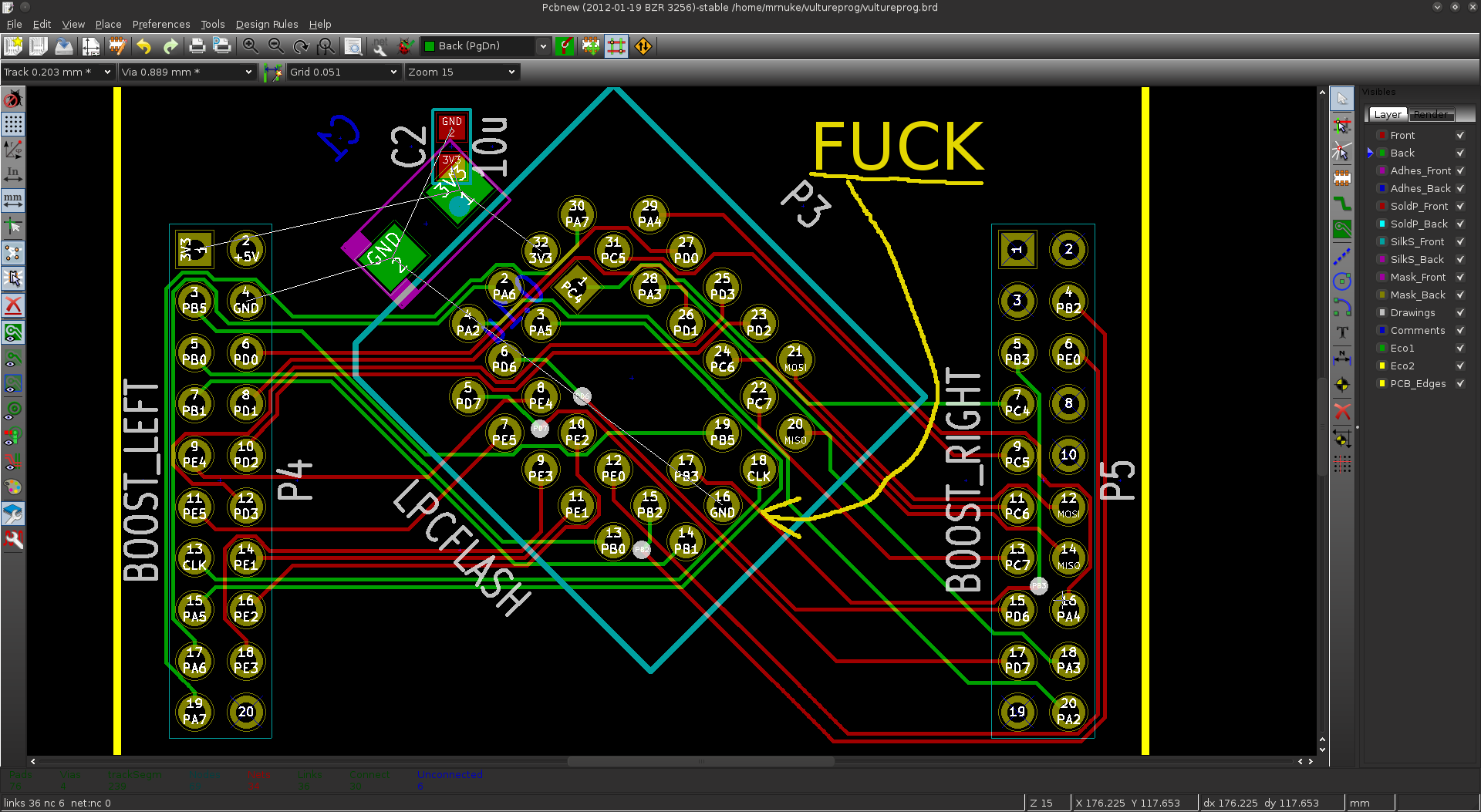
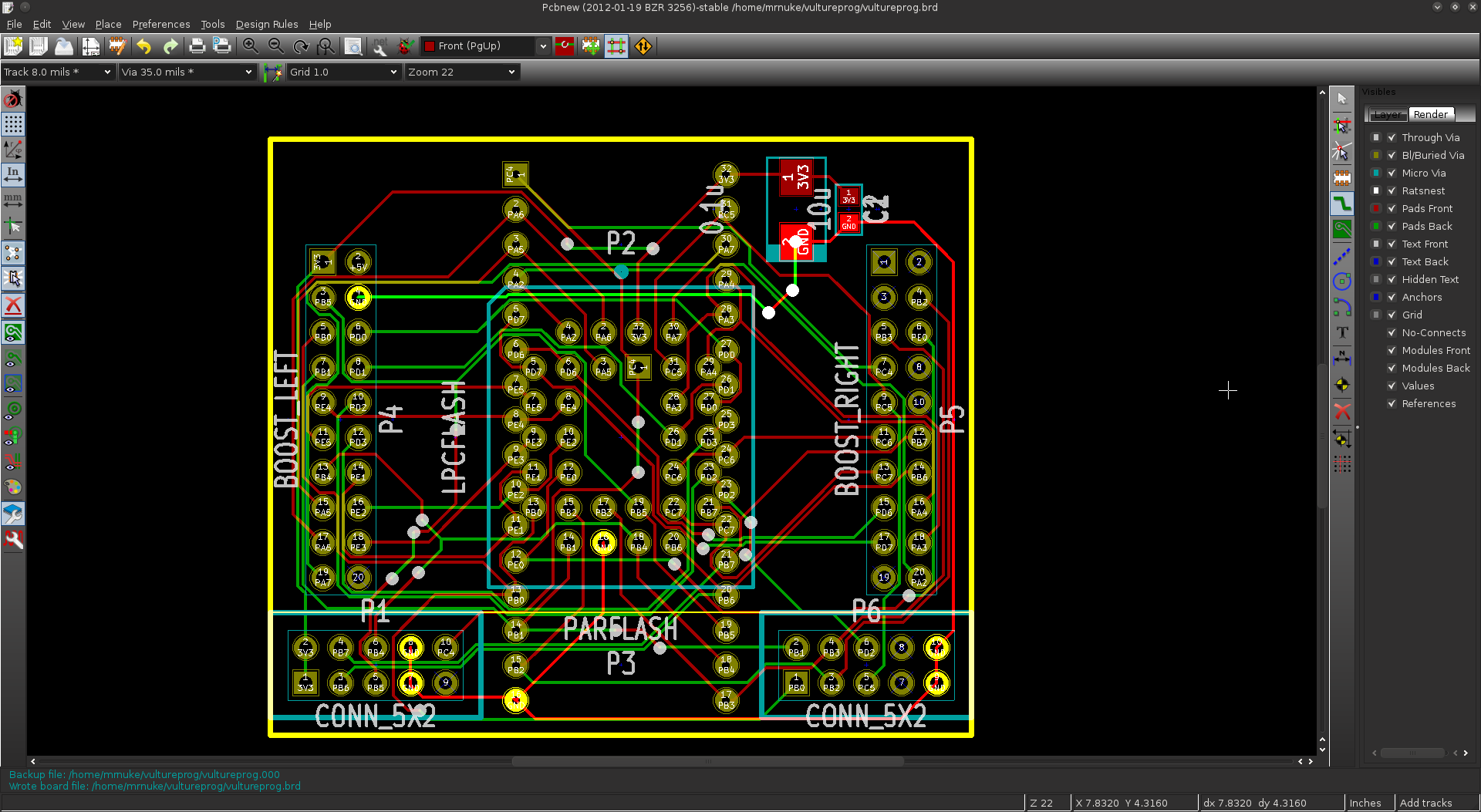
I also wanted to have the option between a normal PLCC32 socket, or a ZIF socket (AKA clamshell). I was really an idiot for thinking I would have both on the same board. On paper, it looks very straightforward. In reality, adjacent pins are on different hemispheres of the globe, and routing them is well, the tastiest spaghetti you have ever eaten. There was no way I could fit both a clamshell, and a PLCC32 socket. There was no way to route the 32 or so tracks on just 2 layers. So I killed the clamshell, the SPI header, and the LPC header. After a couple of hours of messing with the routing, I always had one or two pins that got cornered.
Even routing a simple PLCC socket proved difficult.
What coffee can do to you
I decided to start over, with all the components in place. Once I reduced the track size to 8 mils, and spacing to 6 mils, I was able to route two tracks between a set of pins. This time, I placed the socket inside the clamshell, and managed to connect the two using just the top layer. I then worked from the booster pack connection to the DIP pins on the same side of the board, again, using only the top layer. Then I started using the bottom layer for DIP pins on the opposite side. After a few hours, Chuck Norris warped space and time to make room for all the tracks:
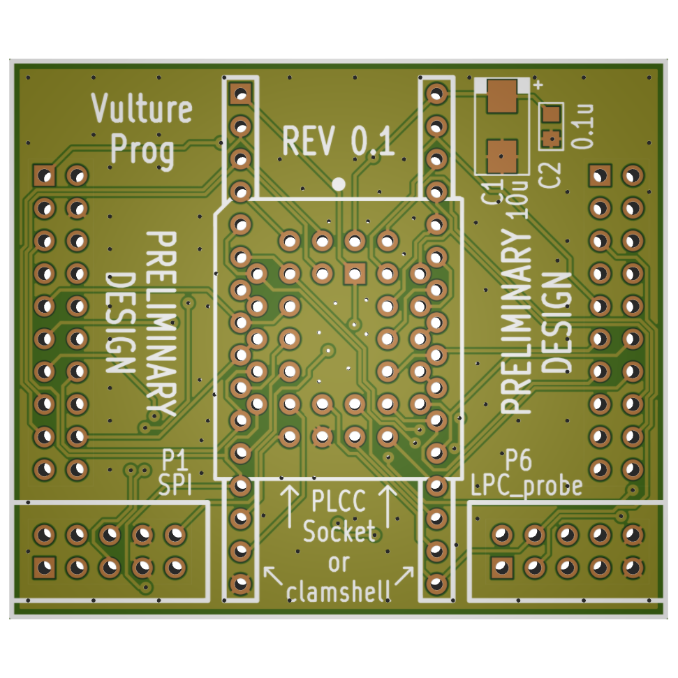
From here, it was a matter of optimizing the routing, taking care of ground planes and other finishing touches. In the end, we get VultureProg hardware version 0.1:
Don’t let the PRELIMINARY DESIGN warning fool you. There is an infinitesimal possibility I will ever want to go back and revise the design. We have 35 GPIOs. accessible on the Stellaris. Five of them are connected to the on-board LEDs and buttons. The remaining 30 are all used up.
Conclusion
If you are a Kicad user, you can head over to yet another one of my GitHub repositories. If you do not have a way to consume Kicad files, you can look in the doc and gerbers directories. Feel free to feed the gerbers to Mayhew Labs’ 3D Gerber Viewer (hint: you can rotate the board in 3D). With all that being done I ordered the first batch of PCBs from Seed Studio’s Fusion PCB service. Routing is definitely too crammed and painful, but I really wanted something versatile and flexible. Whether it lives up to its design goals in REV 0.1 or REV 0.2 remains to be seen. My money is on REV 0.1 — quite literally.


