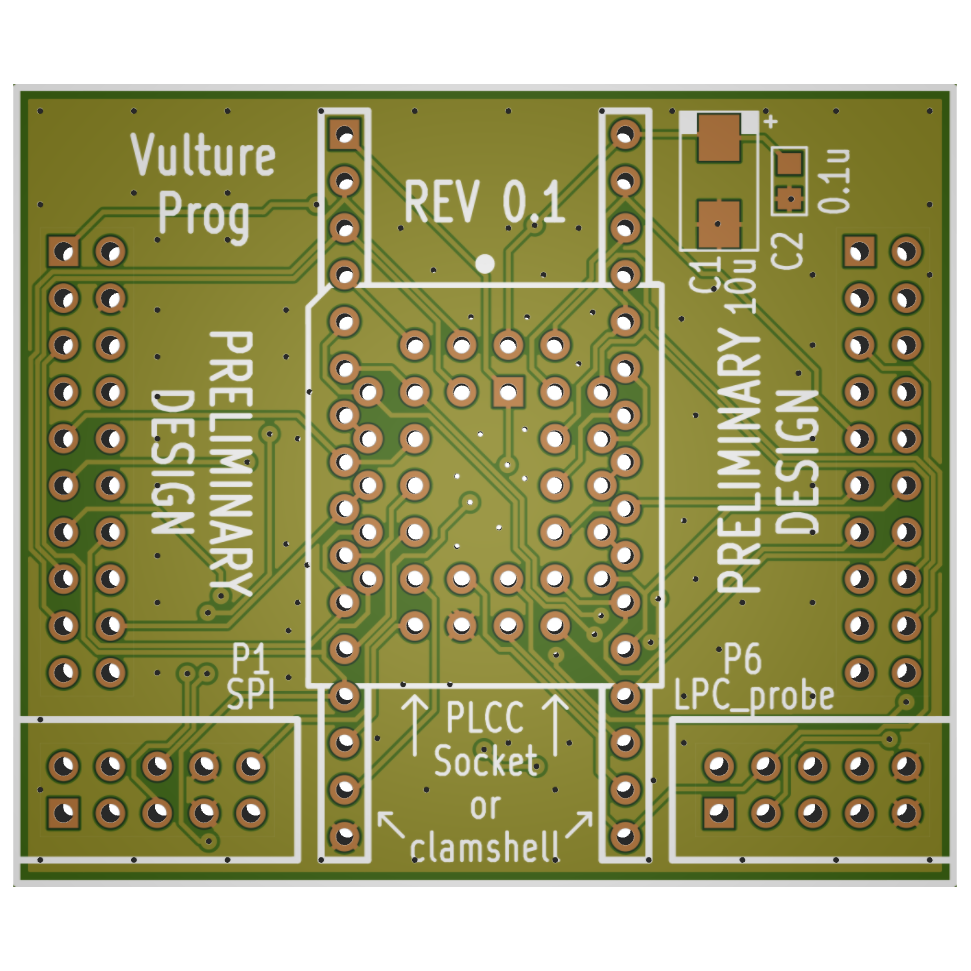
It was time to upgrade. I got a new desk last week. For me, a piece of furniture is as boring as watching stainless steel rust (it does rust eventually). A desk, on the other hand, is anathema to replace. I have 20+ wires connected to my workstation going in all sorts of places. I like to keep these wires carefully routed and out of sight, a task made all the more difficult by the lack of any wire management gizmos on new desks. Consequently, after I get a new desk, you are well within your rights to imagine me grabbing my drilling machine, a set of saw cutter bits and an assortment of hole covers — and you need not wait long to see it. Needless to say, getting back up and running has taken a few days, but we are back with a shiny new VultureProg command center (pictured above for your viewing convenience).
The 80-20 rule
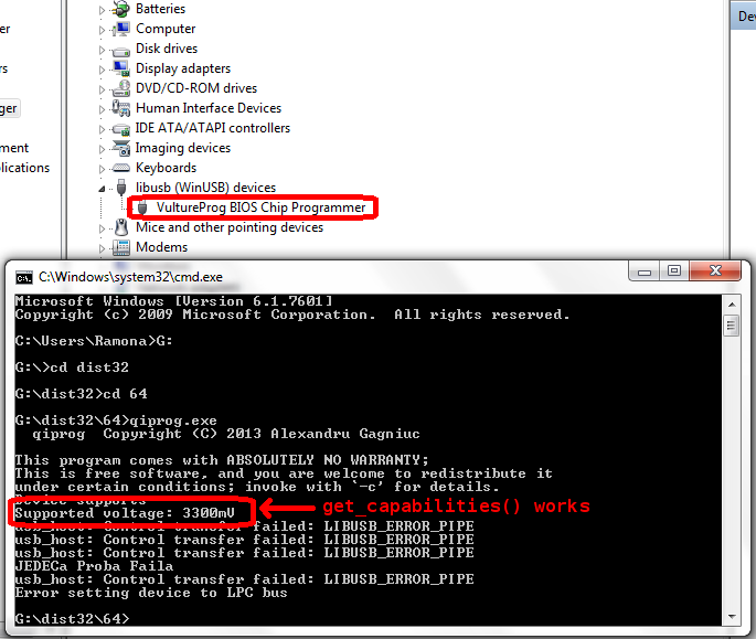
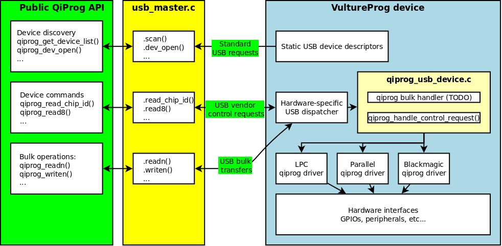
In 2011 I used to work developing Android apps. My boss told me “you will spend 20% of the time writing 80% of the code, and you will spend the remaining 80% of the time writing the remaining 20% of the code”. Sadly, QiProg has proven to not be an exception to this rule. Although I have consistently fixed issues and improved the layout of the code, the number of lines of code has been more or less stagnating after the first three weeks of exponential growth. I know how to erase the chip, I know how to program the chip, I know how to read the chip, and I have code to do all that. I just have not yet had the chance to hook it up to the ecosystem.
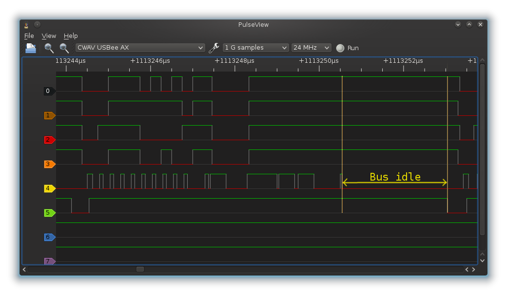
I am currently working on improving the bulk reading code. There are a few corner cases which are not well handled. As expected, it is taking a lot of time, and I even had to write a special testcase before I started.
Did you want fries with that?
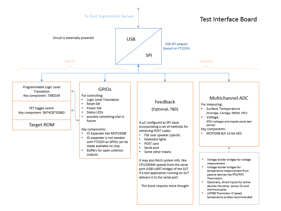
Although we know how to handle every single aspect of the identify/read/erase/write/verify cycle, finding a way of connecting everything together in a simple, elegant, and efficient manner is a different story altogether. We have three API calls for handling erase and write, namely qiprog_set_erase_size, qiprog_set_erase_command, and qiprog_set_write_command. Peter wants everything to work without requiring an explicit erase. In his view, the VultureProg firmware should automatically erase a sector that is being written. Although this would simplify dumb cases where the whole chip or large sections of a chip are written at once, it spells disaster for flashrom’s aggressive optimization. What happens if the first part of a block matches contents, and flashrom decides to write the other part without needing an erase? VultureProg would erase the entire block, then write the second part to the block we never meant to erase. Questions such as this one need to be carefully thought over and elegantly answered. If I blindly start putting all the code together right now, I’ll most certainly have to fix it later.
Postal patronage
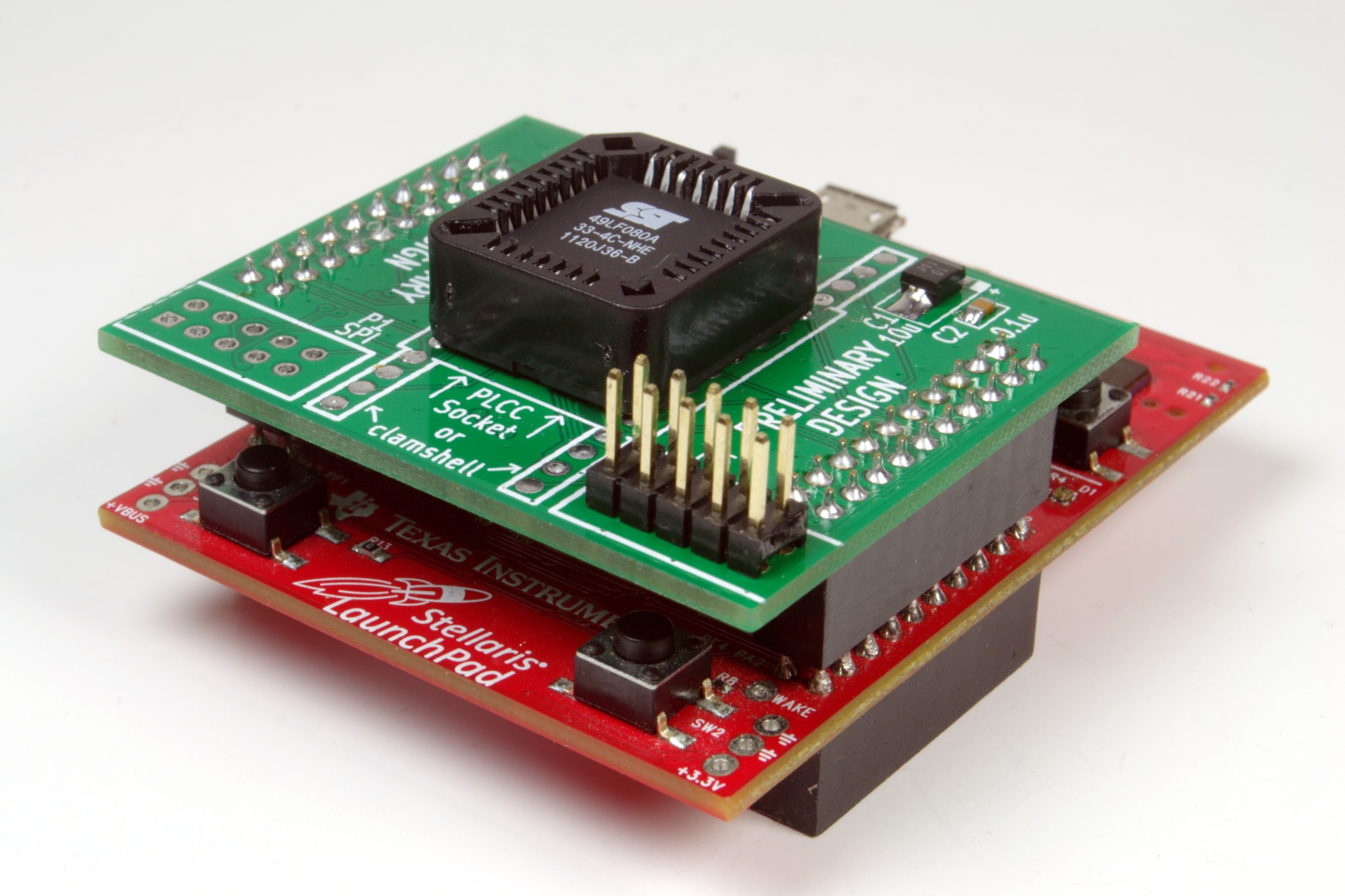
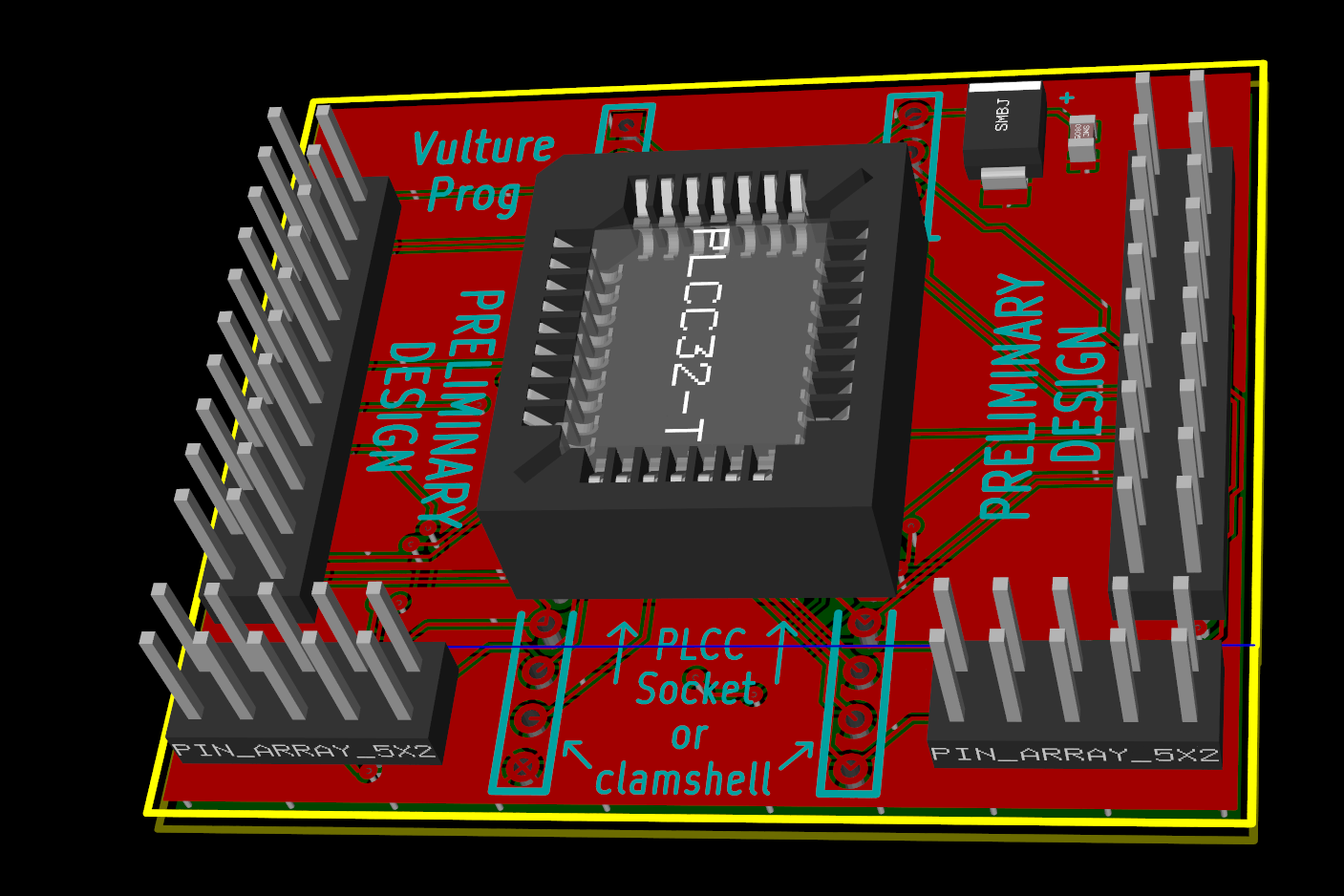
I received a very interesting package last week. I had a deal with Idwer to get him rid of a few LPC and FWH flash chips. I was able to take them off his hands for just a few euros, a deal made sweeter by the fact that those chips are no longer being sold anywhere. I also sent Peter a VultureProg board. Since he already has a Stellaris or two, I have just recruited an eager tester.
Can you send me a board?
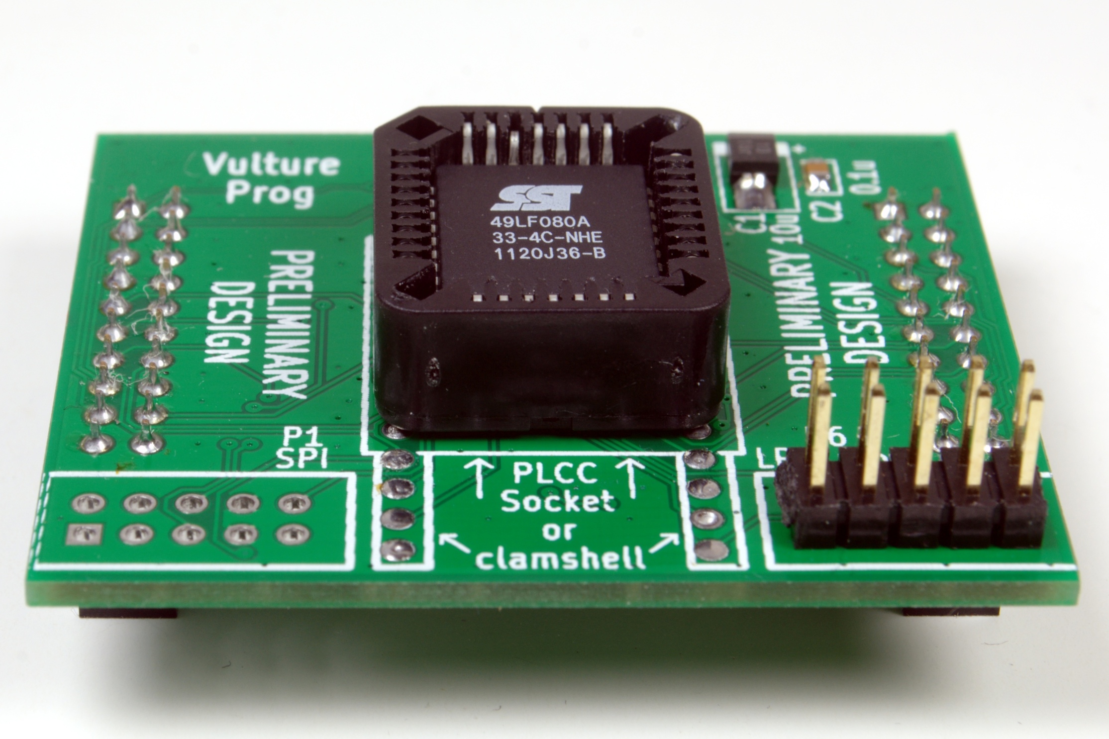
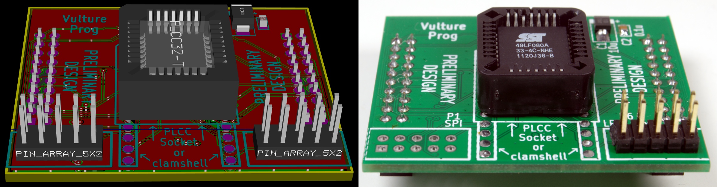
Short answer, no. Just grab the gerbers and take them to SeeedStudio. They will be able to get boards in your hands for much less than what I pay to ship them. The two SMD capacitors are not hard to assemble. If you still want me to send you an assembled PCB, I will charge $50 (international) or $30 (US). I don’t have the physical time to sit and assemble PCBs by hand, plus, it would be very un-geekish of you to not assemble your own.