[GSoC] Better RISC-V Support, week #10

This past week, I worked on the virtual memory initialization code of coreboot on RISC-V. The first part of this was to update encoding.h a file that defines constants such as bit masks which are necessary for interacting with RISC-V’s Control and Status Registers. As a result, I also had to change a few files that relied on outdated constants. Then I wrote some code to walk the page table structures, and fixed one or two bugs in the page table setup code. Unfortunately my patches aren’t as finished as I would like them to be.

When I tested my changes with a Linux payload (which I had to edit the ELF headers of, because Linux uses virtual addresses, while cbfstool and the SELF loader use physical addresses), I stumbled upon another strange error: I get a store access fault in the instruction of the trap handler that saves the first register, even if I initialize the stack pointer to a value that’s within the RAM. When the trap handler runs again to handle this store access fault, it runs without any problems. This fault is especially confusing, because machine mode should always be able to access RAM through its physical addresses.

What’s next?

During the next week, I’ll be traveling and won’t be able to work on coreboot. When I return, I will rework my patches so they can be merged, and hopefully understand the aforementioned access fault problem. Properly set-up page tables should bring me a step closer to running Linux on coreboot/RISC-V (without bbl in the middle).

If time permits, I will start porting coreboot to the Nexys 4 DDR devboard.

[GSoC] Multiple status registers, block protection and OTP support, week #6, 7, 8 and 9

Hello! I have been away for some time now, so this is going to be a longer post. I hope you have missed hearing from me 😛 In this post I will talk about my work in the weeks post-midterm evaluations. After a discussion with my mentors in the midterm evaluations week, we decided to shift focus towards the first three phases of my GSoC proposal for the remainder of the duration. Work on the final phase will be done after GSoC along with the more long-term goals that have come up as I have been making progress.

I submitted patches (finally ;)) to the mailing list. The set of patches adds multiple status register, and block protection infrastructure. I have also added a command-line interface to expose the new functionality. Although I am not sure that the exact wording of the CLI is most optimum, but I did not spend a lot of time on that because IMO it is a rather subjective issue and altering it is not a difficult task. The set of patches also adds support for new infrastructure to around 90 existing chips. I am still waiting to receive feedback and review on them. (My mentors had been slightly busier then.) I am also investigating adding support for access protection to non-SPI chips. This isn’t on the highest priority (more like a long-term goal), but once the SPI infrastructure gets merged, I will begin writing code for that.

Based on the initial prototypes I built (here, here and here), we had decided to use pointers to new structs instead of fully embedding them in struct flashchip. This decision really started to show when I was adding support for existing chips – with only 25 unique struct definitions we were able to support those 90 chips! 😉 One of the problems I faced was that I needed to test the new infrastructure, but doing so on a physical chip would be cumbersome. So that problem was solved by adding a dummy chip to use with flashrom’s dummy programmer. (At that time the code was the dummy chip was messy and something I would be ashamed to put up publicly, but now I have improved upon it! :P)

Currently I am working on finalising the OTP/security register(s) patches – more specifically, adding support to existing chips, code cleanup and documentation. I will be able to send them to the mailing list in a few days. In my research on Eon, GigaDevice and Winbond chips, 2 distinct models for OTP were observed – the GigaDevice and Winbond model with security register(s), and the Eon model with a security sector.

The Security Register(s) model has 3 separate opcodes for read, program and erase – 0x48, 0x42 and 0x44 respectively. A chips can have multiple security registers (most commonly 3, but as high as 4) with each register being anywhere between 128 bytes to 1024 bytes in size (most commonly 512 bytes and then 256 bytes). Usually chips have a lock bit (LB1, LB2, …) in the status register that correspond to respective security registers. These one-time programmable bits are changed using the standard WRSR instruction. Some chips have a single lock bit that controls OTP status for all security registers.

The Security Sector model has a separate sector which can be operated in the OTP mode. OTP mode is entered with opcode 0x3A and exited by sending WRDI (0x04) instruction. While in the OTP mode, the sector behaves just like any other sector – normal read, program and erase instructions apply. The SRP/SRWD bit is served as OTP bit while in OTP mode. Issuing the WRSR command (irrespective of the data sent along with it) will cause the one-time programmable OTP bit to be set.

One of the recurrent issues (for the lack of a better word, I don’t think of it to be an issue really ;)) is that many chips I have based my research on, are not originally supported by flashrom (perhaps unfortunate siblings of the same family that didn’t find support in flashrom earlier xD). I don’t call it an issue per se because after I have submitted my patches flashrom will end up supporting even more chips, but since I have to write more code it might take slightly longer to submit the patches.

There is a third model which is dominantly followed by Spansion chips and a couple of AMIC chips (some AMIC chips follow one of the earlier models – it’s like AMIC couldn’t decide which one to stick to or they probably had different teams working on it! :P). Similar to the security sector design, these chips also have a separate OTP sector but instead of storing configuration in the register, a byte within the sector is allocated for storing the configuration data. I have planned to support this model in the next revision of patches, after the upcoming ones get reviewed and merged.

Thanks for your time, it was nice to get back in touch with you! 🙂
(Phew, that was long! :P)

[GSoC] Better RISC-V support, week #6/7/8/9

Since I haven’t posted an update of my coreboot-on-RISC-V work in a while, this will be a slightly longer post.

Week 6

In week 6, I started documenting how to build and boot coreboot on RISC-V, in the coreboot wiki.
It is now a bit outdated, because we’re moving away from using bbl to boot Linux.

Week 7

I wrote some patches: I removed code that used the old Host-Target Interface (HTIF), because it’s deprecated. I submitted an improved version of my workaround for the bug that causes Spike to only execute 5000 instructions in some cases. I informed the coreboot resource management subsystem about the position of the RAM in physical address space, so that the program loader wouldn’t refuse to load segments into RAM. I submitted two patches to fix compiler errors with the new toolchain.

Meanwhile, there were some good news in the RISC-V world:

Week 8

I submitted a few more patches and started to explore the Nexys4 board. The precompiled bitstream and kernel from the lowRISC version 0.3 tutorial worked without any problems, and after a few days and some help from the lowRISC mailing list, I was able to recompile the lowRISC bitstream.

This week

I discussed the choice of boot medium with the lowRISC developers, and they agreed that a memory-mapped flash would be useful. Once it is implemented, I
can start porting coreboot to lowRISC on the Nexys 4 DDR board. Luckily the Nexys4 already has large enough flash to use for this purpose.

My mentors and I agreed that the switch from machine mode to supervisor mode should be left completely to the payload.

What’s next?

I will continue to work on running coreboot on the Spike emulator. Currently I’m facing the following problems and tasks:

  • Linux, when compiled to an ELF file (vmlinux) specifies that it wants to be loaded at the physical address 0x0 and at the virtual address 0xffffffff80000000. Since coreboot’s ELF loading code only looks at the physical address, it refuses to load Linux, since RAM starts at 0x80000000 on RISC-V.
  • Low level platform information (most importantly the memory layout) is passed to the firmware (coreboot in this case) as a configuration string, which is dynamically generated by the emulator, in the case of Spike. I still need to implemented a parser for this format, so coreboot can know how much memory is available.
  • The RISC-V Privileged Architecture Specification 1.9 specifies that there shall be a page at the top of the virtual address space where the operating system can call a few functions exposed by the firmware (this is the Supervisor Binary Interface).

[GSoC] Better RISC-V support, week #4/5

Week 4

In week 4, I tracked down why coreboot halted after about one line of output. It turned out to be a spike bug, that I wrote up in this bug report, and affect any program that doesn’t have a tohost symbol. As a workaround, I extended my script that turns coreboot.rom into a ELF to also include this symbol.

After some more patches I could run coreboot in spike and get the familiar “Payload not loaded” line.

Week 5

I was now clearly moving towards being able to run linux on spike/coreboot. But there was a problem: The RISC-V linux port requires a working implementation of the Supervisor Binary Interface (SBI), which is a collection of functions that the supervisor (i.e. the linux kernel) can call in the system firmware.

Coreboot has an implementation of the SBI, but it’s probably outdated by now. To get an up-to-date SBI implementation, I decided to use bbl as a payload. When I built bbl with coreboot’s RISC-V toolchain, I noticed that it depends on a libc being installed in two ways:

  • The autoconf-generated configure script checks that the C compiler can compile and link a program, which only succeeds if it finds a linker script (riscv.ld) and a crt0.o in the right place.
  • bbl relies on the libc headers to declare some common functions and types (it doesn’t use any of the implementations in the libc, though).

The coreboot toolchain script doesn’t, however, install a libc, because coreboot doesn’t need one.

I tweaked the bbl source code until it didn’t need the libc headers, changed the implementation of mcall_console_putchar to use my 8250 UART, got the payload section of bbl (where linux is stored before it’s loaded) out of the way of the CBFS by moving it to 0x81000000 (bbl/bbl.lds is the relevant file for this change), and could finally observe Linux booting in spike, on top of coreboot and bbl. It stops with a kernel panic, though, because it doesn’t have a root filesystem.

Plans for this week

This week I will document my work on the Spike wiki page in the coreboot wiki, so others can run coreboot on spike, too.

[GSoC] Better RISC-V support, week #3

Last week, after updating GCC (by applying Iru Cai’s patch) and commenting out uses of outdated instructions and CSRs (most notably eret and the HTIF CSRs), I noticed that coreboot crashed when it tried to access any global variables. This was because the coreboot build system thought coreboot would live near the start of the address space.

I found spike-riscv/memlayout.ld, and adjusted the starting offset. But then I got a linker error:

build/bootblock/arch/riscv/rom_media.o: In function `boot_device_ro': [...]/src/arch/riscv/rom_media.c:26:(.text.boot_device_ro+0x0): relocation truncated to fit: _RISCV_HI20 against `.LANCHOR0'

I played around with the start address and noticed that addresses below 0x78000000 worked, but if I chose an address that was too close to 0x80000000, it broke. This is, in fact, because pointers to global variables were determined with an instruction sequence like lui a0, 0xNNNNN; addi a0, a0, 0xNNN. On 32-bit RISC-V, the LUI instruction loads its argument into the upper 20 bits of a register, and ADDI adds a 12-bit number. On a 64-bit RISC-V system, lui a0, 0x80000 loads 0xffffffff80000000 into a0, because the number is sign extended.

After disassembling some .o files of coreboot and the RISC-V proxy kernel, I finally noticed that I had to use the -mcmodel=medany compiler option, which makes data accesses pc-relative.

Now that coreboot finally ran and could access its data section, I finished debugging the UART block that I promised last week. Coreboot can now print stuff, but it stops running pretty soon.

Plans for this week

This week I will debug why coreboot hangs, and will hopefully get it to boot until the “Payload not found” line again, which worked with an older version of Spike.

Also, Ron Minnich will be giving a talk about coreboot on RISC-V at the coreboot convention in San Francisco, in a few hours.

[GSoC] Multiple status registers, block protection and OTP support, week #1 and #2

Hi, I am Hatim Kanchwala (hatim on IRC) from India. I am the GSoC student working with flashrom this year. Stefan Tauner (stefanct) and David Hendricks (dhendrix) will be mentoring me (thanks a lot for the opportunity). The pre-midterm phase of my project comprises three sub-projects – multiple status registers, block protection and OTP support. Each of these projects deals with SPI flashchips.

As of writing this post, flashrom supports over 300 SPI flashchips. Around 10% have multiple status registers (most have two but there is one with three). Almost all have some sort of block protection in place. Around 40% have some variation of OTP or security registers. A combination of BP (Block Protect, first status register) and SRP bits (usually first, but sometimes second status register as well) in the status register determine the range and type of protection in effect. A few have a TB bit (Top/Bottom) in addition to BP bits. Some also have a CMP bit (Complement Protect, second or third status register) to add more flexibility to range available. Few chips have a WPS bit (Write Protect Scheme, second or third status register) that define which scheme of access protection is in use. Chips with security registers have corresponding LB bits (Lock Bits, second status register) which are one-time programmable and, when set, render the corresponding security register read-only. Chips with a separate OTP sector(s) have opcodes to enter/exit OTP mode and, within OTP mode usual read, page program and sector erase opcodes can be used.

Previously, flashrom could only read/write the first status register. For writes, all block protect bits were unset (this configuration corresponds to block protection), if the type of protection allowed it. Once unset, flashrom couldn’t revert the BP bit configuration. The ChromiumOS fork of flashrom has some support for locking/unlocking block access protection in place. A lot of the work is done around specific families of chips, but they are moving towards generalising it. For chips with OTP support, flashrom simply printed a warning.

In these two weeks I sifted through around 5-6 dozen datasheets and developed models for multiple status registers, block protection and OTP/security registers. I discussed with mentors and the community over mailing list (link to thread) the infrastructural changes and use cases corresponding to the models. To substantiate these ideas, I wrote separate prototype code. In the process, Stefan introduced me to a powerful tool, Coccinelle. This tool will make applying changes to the large struct flashchips easier while being safe. As a byproduct of studying existing flashrom infrastructure, I had the opportunity to explore the history of flashrom through git log – evolution of flashrom from its humble beginnings in coreboot/util to flash_and_burn to flash_rom to finally flashrom today!

My broad targets for the following few weeks will be to finish up with the pending dozen or two datasheets, polish the models and start transforming the prototype code into merge-worthy code. Following the infrastructure changes, I will update existing chips to make use of the new infrastructure, add support for a bunch of new chips and finally test on actual hardware.

Thanks. See you later!

[GSoC] Better RISC-V support, week #2

Last week, I updated my copy of spike (to commit 2fe8a17a), and familiarized myself with the differences between the old and the new version:

  • The Host-Target Interface (HTIF) isn’t accessed through the mtohost and mfromhost CSRs anymore. Instead, you have to define two ELF symbols (tohost and fromhost). Usually this is done by declaring two global variables with these names, but since the coreboot build system doesn’t natively produce an ELF file, it would get a little tricky.
  • Spike doesn’t implement a classic UART.
  • The memory layout is different. The default entry point is now at 0x1000, where spike puts a small ROM, which jumps to the start of the emulated RAM, at 0x80000000. One way to run coreboot is to load it at 0x80000000, but then it can’t catch exceptions: The exception vector is at 0x1010.
  • Within spike’s boot ROM, there’s also a text-based “platform tree”, which describes the installed peripherals.

“Why does coreboot need a serial console?”, you may ask. Coreboot uses it to log everything it does (at a configurable level of detail), and that’s quite useful for debugging and development.

Instead of working around the problems with HTIF, I decided to implement a minimal, 8250-compatible UART. I’m not done yet, but the goal is to use coreboot’s existing 8250 driver.

Plans for this week

This week, I will rewrite the bootblock and CBFS code to work with RISC-V’s new memory layout, and make sure that the spike UART works with coreboot’s 8250 UART driver. Booting Linux probably still takes some time.

[GSoC] Better RISC-V support, week #1

Hi, I’m Jonathan Neuschäfer (jn__ on IRC) and my GSoC project for this year is to improve coreboot’s support for RISC-V platforms. RISC-V is a new instruction set architecture (ISA) that can be implemented without paying license fees and is relatively simple.

Coreboot has already been ported to RISC-V in 2014, and has since received a bunch of patches, but since the RISC-V Privileged ISA Specification (which defines things like interrupt handling and virtual memory) is still in flux, it has become unbootable again.

My first first goal last week was to run coreboot in SPIKE, the official RISC-V emulator, and get some console output. I checked out commit 419f1b5f3 (current master) of the riscv-tools repository and built SPIKE from there.

After I patched a few outdated instructions and worked around the fact that the RISC-V binutils port currently included in coreboot targets a newer version of the RISC-V Privileged Spec by hardcoding some Control and Status Register numbers, I finally got coreboot booting until the point where it would jump into a payload, had I specified one.

All patches can be found under the riscv topic on gerrit.

Plans for this week

This week I will update my SPIKE to a version that supports the upcoming Privileged Spec 1.9, which will be released in the next couple weeks. This has the advantage that I don’t need to patch instructions because GCC encodes them differently than SPIKE decodes them. Additionally, I’ll try to get Linux to boot in SPIKE, under coreboot.

[GSoC] EC/H8S firmware week #7|#8

Week #7 was is little bit frustrating, because of no real progress, only more unfinished things which aren’t working. Week #8 was a lot better.

1. Sniffing the communication between the 2 embedded controllers H8S and PMH4.

I’ve tried to build an protocol analyser with the msp430, but the data output was somehow strange. For testing purpose I used my H8S firmware to produce testing data. But the msp430 decoded only wrong data. I’m using IRQs on the clock to do the magic and writing it to a buffer before transmitting it via UART. Maybe the msp430 is too slow for that? Possible. Set a GPIO to high when the IRQ routing start and to low when it ends. Visualize the clock signal and connect the  IRQ measure pin to an oscilloscope. The msp430 is far too slow. I’m using memory dereference in the IRQ routine, which takes a lot of time. Maybe the msp430 is fast enough, when using asm routine and registers to buffer the 3 byte transmission. But a logic analyser would definitely work. So I borrowed two logic analyser. An OLS (Openbench Logic Sniffer) and a Saleae Logic16.

There isn’t so much data on the lines. Every 50 ms there is a short transmission of 3 byte. But I don’t want to decode the data by hand. So it needs a decoder for the logic analyser. sigrok looks like the best start point and both analyser are supported.

I’ve started with the Openbench Logic Sniffer, but unfortunately it doesn’t have enough RAM to buffer the input long enough. Maybe the external trigger input can be used. But before doing additional things I would like to test with the Logic16.

The Logic16 doesn’t support any triggers but it can stream all data over USB even with multiple MHz. Good enough to capture all data. I found out that the best samplerate is 2 MHz. Otherwise the LE signal isn’t captured, because it’s a lot shorter than a clock change. In the end I created a decoder with libsigrokdecode.

sigrok-cli -i boots_and_shutdown_later_because_too_hot.sr –channels 0-3 -P ec_xp:clk=2:data=3:le=1:oe=0 | uniq -c 

67 0x01 0x07 0xc8
3 0x01 0x04 0xc8 
4 0x01 0x10 0x48
1120 0x01 0x17 0x48
67 0x01 0x07 0xc8

0x01 0x07 0xc8 is called when only power is plugged in, like a watchdog(every 500ms)
0x01 0x17 0x48 is called when the device is powered on, like a watchdog (every 50ms)
0x01 0x04 0xc8 around the time power button pressed
0x01 0x10 0x48 around the time power button pressed

2. Flash back the OEM H8S firmare

The OEM H8S firmware is included in the bios updates. cabextract and strings is enough for extracting it out of the update. Look for SREC lines. Put the SREC lines into a separate file and flash them back via UART bootloader and the renesas flash tool. The display powers up and it’s booting again with OEM BIOS.
I could imagine they are using a similar update method like the UART bootloader. First transfer a flasher application into RAM and afterwards communicate with the flasher to transfer the new firmware, but the communication works over LPC instead of UART.

3. Progress on the bootloader

I’ve implemented the ADC converter to enable the speaker amp and the display backlight brightness.

Written down LPC registers and just enable the Interface in order to get GateA20 working. Still unclear how far this works.

4. How to break into the bootloader?

The idea of the bootloader is providing a brick free environment for further development. The bootloader loads the application which adds full support for everything. It should be possible to stop the loading application and flash a new application into the EC flash. When starting development on the x60 or x201 I want to use I2C line as debug interface. I2C chips have a big footstep and are easy to access. But there must be a way to abort the loading. I will use the function key in combination with the leds.

  1. Remove the battery and power plug.
  2. Press the function key
  3. Put the power plug in
  4. Wait until leds blinking
  5. release the function key within 5 seconds after the leds starting to blink to enter the bootloader.

The H8S will become I2C slave on a specific address.

What next?

  • Add new PMH4 commands to the H8S
  • solder additional pins to MAINOFF PWRSW_H8 A20 KBRC
  • use the logic analyser to put the communication in relation with these signals
  • UART shell
  • I2C master & client
  • solder LPC pins to analyse firmware update process
  • test T40 board with new PMH4 commands and look if all power rails are on

[GSoC] EC/H8S firmware week #6

This week I looked at the communication between the EC H8S and the PMH4. The PMH4 (likely power management hub) is an ASIC which takes care of the power control. It controls who get’s power and who not. It doesn’t do any high level work, more like a big logic gatter. The PMH4 has inputs from several power good pins from different power rails and chips. On the output side it controls some power rails. It can also reset the H8S. The PMH4 also knows over some pins in which power state (ACPI S0,S4,S5) the board is. It doesn’t do any high level work. It’s more like a big logic gatter. There are no ADC on any power lines.

The PMH4 is connected to the H8S via 4 Pins. ~OE LE DATA CLK.

gsoc 2015 pmh4 connector t40

I connected a buspirate in SPI sniffer mode to debug the protocol. But the output looked a little bit strange. There was no data from the PMH4 to H8S (MISO) and the data comes in burst. To get more knowledge on the protocol I used a digital oscilloscope.

pmh4 oscilloscope

The protocol doesn’t look like SPI. LE get’s low after every transmission, ~OE is just high, clock and data just transfer the data. Sometimes when the H8S gets an interupt the Clock pause for some time and continues with the data afterwards. The clock is around ~400kHz.

I confirmed the protocol via the oscilloscope, but still I don’t get any sign from the board. No fan, nothing else. There must be more than this single transmisison. Maybe the board is to much damaged. My modified board was already broken when I got it. There is a loose connection related to the cardbus. Maybe this is my problem I don’t know.

I’ve two board with two connectors for the PMH4 here. Why not using the OEM one as starter help for the other one?

t42 gives some starting help

I think the PMH4 does what it should do. The H8S has an digital-analog-converter pin connected to the video brightness. But I haven’t implemented it yet. But I don’t think the device booted, because neither the CPU nor the chipset produce any heat. Ok, maybe it does, I only used my finger as thermometer. A thermal camera would help here. I’ll borrow a thermal camera for that.

There are lot of pins which I ignore atm. E.g. A20 pin. Is there something to do in a specific time serie?

What’s next?

  • build a small protocol sniffer for the PMH4 XP using a msp430 or stellaris arm
  • make progress on the bootloader
  • find a way to flash back the OEM H8S firmware
  • find a way to flash my bootloader via OEM flash tools

My requirements to the bootloader are

  • UART flashing via XMODEM
  • a simple UART shell
  • I2C as recovery and shell as well

I2C pins are a lot easier to find and modify than the H8S UART. I’m not yet sure if the H8S should be the master or the slave and on what address he should use? Multiple? UART tx is working. Rx is a task to do.

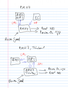
PMH4 / PMH7 / Thinker communication

On newer board the PMH interfaces changed (>= x60, t60, …). They merge the LPC interface and the XP interface into an protocol over SPI. And the new PMH is used as GPIO expander as well.

pmh4 pmh7 thinker communication