[GSoC] EC/H8S firmware week #5

The T40 is flashing leds! The toolchain is still a little bit tricky. I’m using the debian package gcc-h8300-hms, written a small linker script and took the startup assembly routine from Johann Gysin’s led radiator.

Now I can flash leds. But what about booting the board? I would say it’s enough to put

  • (!MAINOFF) = high
  • FAN ON = high
  • pulse high on (!PWRSW_H8)

But it’s not enough. Also the FAN isn’t starting to rotate. I’ll try to debug every pin this week and solder some debug pins for the 2nd EC (PMHx) to the my modified T40 as well as to an unmodified T42p. The H8S is talking to the PMHx via SPI, while the H8S is the master and is doing bit banging SPI in software, because it doesn’t have a hardware unit for that. I’ll also use these pins for testing my SPI implementation. I’ll try to reuse an open source SPI implementation.

I also asked me if it’s a good idea to port coreboot for the T40 before continuing any efforts to the EC, but it’s a little bit harder, because the T40 uses a LPC/FWH flash in a TSOP40 case. Another option is changing the hardware to a board which is already supported by coreboot like a x60/t60 or x201. But it’s much more harder to access the 8 pins for flashing the EC on these boards.

Before switching to another board, the powersequencing must work and I need a robust recovery way, because when you kill the EC by flashing a new firmware, you don’t get a second chance, unless you solder a lot. Chrome EC fix this problem by splitting the EC firmware into 2 parts. One read-only part and one read-write’able part. Only the second part gets updated and the read-only part can at least boots the device.

Before starting the H8S port for Chrome EC I want to have a bootloader. Because it would improve developing speed. I think implement this is much faster than doing the full Chrome EC support and most of the bootloader code can be re-used for Chrome EC.

I’m also not perfectly sure Chrome EC is the best solution. It’s special use-case is EC, which is perfect. But neither the documentation (I think there is more than one page) nor the bugtracker is public. Thus it makes difficult to use. I’m also not sure if Chrome EC would apply my H8S port into their repository.

[GSoC] EC/H8S firmware week #3|4

In the last 2 weeks I managed to flash the H8S on the T40 using the OEM Renesas Flash Tool including their flash application. Flashing works in 2 steps, first upload a flash application into the H8S. Second this flash application will receive the firmware (via serial) and write it into the flash. Thanks to Renesas this application is available in source code. I would like to write an own flasher later.

But I wasn’t able to create a proper application yet. I could write the led programm in assembly, but having a working c compile is needed anyway.

I built a toolchain with gcc 4.9.2. The toolchain buildscript is very simple and can be found on github. I stopped my building efforts for now (building one based on gcc 4.4.6). There’s also a debian package for h8300 (based on gcc 3.4.6) which may be a good alternative. Before continuing in building toolchains and my led application, I’m reading me into linkerscipts and take a look how the compiler is working (e.g. what must a crt0 do?).

At the moment I know how the application should be compiled, where the reset vectors are and where the entrypoint. But putting these things together into a binary image is my task now.

The dev board I mentioned in my last post was stuck by the german post for the last 2 weeks, because there were on strike. The board is now in the custom office and I’ll collect in the next days, which will takes severals hours in Berlin.

[GSoC] EC/H8S firmware week #2

The last week was a little bit depressive. I did the some resoldering. Pin P90 wasn’t connected to 3.3V which is needed to enter the flash boot mode. It was soldered  to the VCC of the Serial level shifter MAX3243. After searching some minutes with the Multimeter for a better power source, I decieded to use 3.3V near the H8S. It’s now a very long cable across the board.

Now let’s see, how good this works? Nothing :(. Recheck with a voltmeter and found another problem with P91 (/SUS_STAT). When connecting SUS_STAT with an 1k resistor to 3.3V the voltmeter shows 0.04V. This means it’s driven by something else to 0V. My hope was that the chipset isn’t driving this until it’s powered. But sadly it is driving it to 0V. What’s SUS_STAT? SUS_STAT can be used as LPCPD (LPC power down) and is used to notify devices to enter a low power state soon. Suspend Status is active low, which means all device should be in low power mode.
What should I do now? I need 3.3V on that line.

There are multiple solution:

  • Remove 1k and burn it to death. But likely this could kill the chipset or
    a least this certain pin or multiple pins
  • Cut the pin
  • Bend the pin upwards while desoldering
  • Desolder the whole chip and bend afterwards, resolder
  • Replace the chip with a socket (expensive and rare)

This decision is not easy to take, especially because I never done most
of these things. This got me stuck for a while until Peter helped me out,
he bend a single pin upwards. Thanks!

The next week milestone is still flashing the EC, the same goal since the first week. So the time schedule will be a little big chaotic. Maybe I can hurry up and reach another weekly goal fast than a week.

Because I was stuck on that a little bit, I took another look on ebay and bought a development board with a H8S/2633. 2633 is a little bit newer than the 2100 series
which is used in Lenovo laptops. The board should arrive in one week, but atm it’s in german customs. Such development boards are hard to get for a “good” price. Brand new boards start with several hundred euros or dollars. E.g. the debugger E10 (USB device) cost around 1000 Euro, it’s only a stupid USB device. I already bought on ebay an E8, previous generation debugger, but it can not debug the chip, only flash them with the Renesas software/IDE.

Beside my project I’ve done some other work on coreboot. I helped Holger Levsen on creating a reproducible build job for coreboot on reproducible.debian.net. More info about reproducible builds are on their wiki page.  To improve reproducibility I created 2 patches #10448 #10449. They cleaned up reproducible bugs in coreboot and without building Payloads, most targets are now reproducible. Great thanks to Holger Levsen for his work on that!

[GSoC] EC/H8S firmware week #1

The first task of my project is a working development board. A development board means that I have serial communication and I can flash new firmwares the chip and whole mainboard isn’t booting. The chip is a H8S 16-bit microcontroller with 64kb to 128kb EEPROM and is available in different packages. BGA and TQFP. BGA means the pins are under the chip, TQFP has pins on the side. TQFP is nice to hack, but most modern Thinkpads use the BGAs. But a T40 or T42 use a TQFP package. A friend donated his old T42 to me! Thanks a lot! Now with a hackable T42 I can start to create a development board out of the T42 mainboard. Like most other microcontroller this chip has a programmable bootloader in a ROM (called rom loader). The bootloader can boot to different states, configurable via 5 pins (MD0 MD1 P90 P91 P92).
P90 to P92 are only read when MD0 and MD1 are in a special bootstate.
After reading the documentation I found that the pins must match the following volatage levels to select the flash boot mode:

MD0-MD1 = 0V, P90-P92 = 3.3V.

Besides these configuration pins we need some additional wires to the following pins:
/RES – reset active low
UART RX – serial communication
UART TX –

Now it gets interesting. The MCU (microcontroller unit) can use a pin for different purposes depending on the PCB designer. Those pins called multifunction pins. Hopefully we don’t get blocked by unaccessible pins. After reading more documentation and using a Multimeter on the board I found out that /RES, RX, TX, MD1 require soldering, but are easy accessible. MD0 is already in a good state.
P90 is connected via a resistor to ground, but we need it to 3.3V.
Let’s find the resistor to solder 3.3V to it… Mhh. tricky! 3h later I found it on the
board hidden under the PMH4 (2nd EC/GPIO expander). Very uncommon.

P91 is named /SUS. Suspended active low, but can be driven by multiple controllers (chipset + h8s).
Because we want to boot linux on the main cpu later in the project we should not kill the chipset. I added a pin connector to this pin.

And the last pin P92 was connected to the SuperIO UART’s level shifter (MAX3242). I had to desolder the chip because P92 was driven by the level shifter.

Near the EC are 2 testpoints which are connected to an I2C bus. I soldered these too, because an I2C could be useful.

1 P91
2 GND
3 md1
4 /RESET
5 RX
6 TX
7 I2C SDA
8 I2C SCL
+
1 patch cable with a 3.3V + 1k Resistor (for P91).

So far so good. But somehow it doesn’t work. Some pins doesn’t have the right level. P92 doesnt have 3.3V. Why not?
P92 is pulled up via a resistor to VCC of the TTL shifter. The VCC isn’t powered. I need to resolder it to another 3.3V pin somewhere and take another look
on the other levels too.

PS. Some work was already done before GSoC started. I posted the first part of soldering on my blog

coreboot GSoC 2015

coreboot has been accepted as a mentoring organization for GSoC 2015! We are accepting student applications for coreboot, flashrom, and SerialICE projects.

Students:  Welcome! Please review the coreboot GSoC page and Project Ideas page. Student applications formally open on 16 March at 19:00 UTC.

Mentors:  Please signup in Melange and request to join the coreboot project. You must signup for 2015, even if you already have a Melange account. You may also find the GSoC Mentor Guide helpful.

Community:  Please recruit and welcome prospective students to the organization. You may provide ideas on the Projects Page.

GSoC 2014 Projects

Congratulations coreboot’s GSoC students.  coreboot has three students working on coreboot for GSoC 2014 .


Title: Enhance early coreboot debugging

Student: Kyösti Mälkki

Mentors: Martin Roth and Rudolf Marek


Title: Generic Interface using alternate CBFS access patterns for ARM SoCs

Student: Naman Govil

Mentors Aaron Durbin and Marc Jones


Title: The yearly flashrom maintenance and enhancement proposal

Student: Stefan Tauner

Mentors Carl-Daniel Hailfinger and David Hendricks


Each student is required to post progress to this blog.  We expect first posts later this week. Stay tuned for progress!

GSoC (coreboot): Test interface board complete

Apologies for the late update. The design that I posted in the last post was more challenging than I had thought. However I’m happy to announce that my test hardware that I call ‘coreboot test interface board’ (TIB) is now complete. Only some of the software interface part is remaining in the project. So let me share with you a very quick update of last month. Continue reading GSoC (coreboot): Test interface board complete

GSoC (coreboot): Week 5-7 – Redesigning the test-interface-board

In the last blog post I talked about the test-interface-board. There were some concerns about the use of FT232H chip and extra features like voltage and temperature measurement were not required. Keeping in view all the suggestions and improving things on my side I have redesigned the board.

w567fig1

The figure above shows only one target board connected to the test supervision for simplicity. The purple L-block is the test-interface-board. This time, instead of using an integrated flasher I wish to support all existing flashers so I have developed an ICP adapter. An In-Circuit Programming (ICP) adapter contains the firmware flash memory removed from the motherboard and it acts as an electronic change-over switch that connects this flash memory to the motherboard or the programmer as required. It also includes logic-level translation to support as many as possible combinations of programmers and motherboards. The support for programmer voltage is in range 1.2V-5.5V and for motherboard SPI voltage it’s in range 1.65V-3.3V.

As a quick test for VGA initialization I’ve added video detection for Analog video (VGA), DVI and HDMI ports. This checks presence of signals that are only there when video is active. In other words, it checks whether a monitor’s status led would turn green if it’s plugged to the motherboard without actually plugging one. I have prepared schematics, some parts of which are yet to be validated through prototyping. This will all be implemented as an Arduino add-on board (aka Shield) for convenience and the Arduino would act as the controller.

The Serial and Ethernet ports can be connected in the usual way using Serial-to-USB cables, Ethernet cables and hubs. Continue reading GSoC (coreboot): Week 5-7 – Redesigning the test-interface-board

GSoC (coreboot): Week 3 and 4

In the past two weeks I was on vacation and I have been working on what I call “test interface board”. Before I go on to elaborate this I feel there’s a need to discuss the big picture of this project because a lot of things have changed for good reasons and the old terminologies don’t make sense.

System Topology

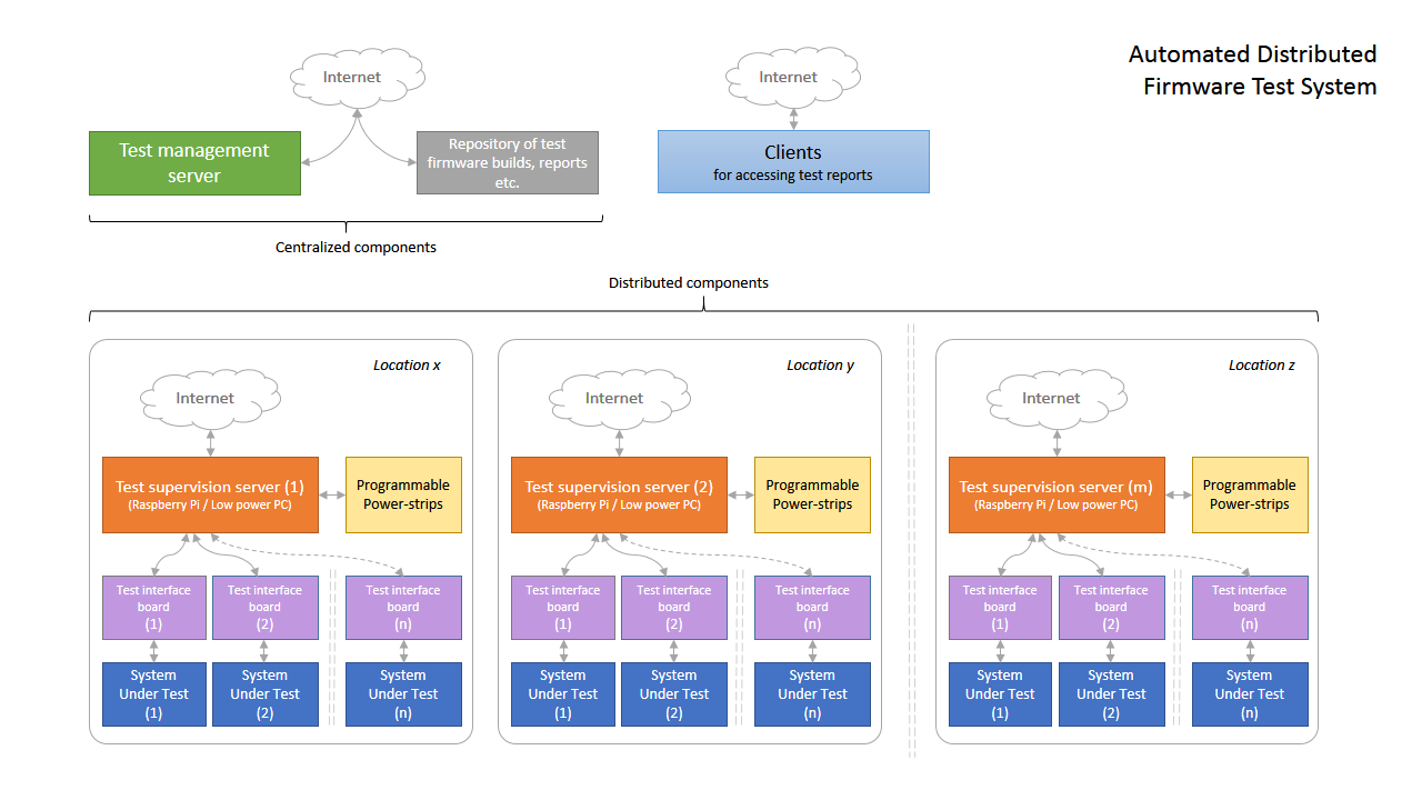
Just to remind, my project is centered on building inexpensive and flexible test-rig for the Automated Distributed Firmware Test System described in Quality Assurance Talk by Stefan Reinauer.

A centralized Test Management Server generates test sequences for remotely located systems under test (SUTs) and this includes controlling and monitoring the SUTs and flashing different firmware builds on them. The test management server coordinates with a repository for accessing test builds and for storing test reports. Test reports are the final and useful output of the whole system and these may be accessed using browser by clients from internet.

A Test Supervision Server is a low power computer that acts as a local housekeeper of SUTs for a given physical location. It connects to the Test Management Server using SSH over internet and executes given test sequences by coordinating closely with the SUTs using a Test Interface Board. Programmable power-strips are provided to control power supply to the SUTs from Test Supervision Server.

My work will be confined to the distributed components for now. I have completed the programmable power-strip block. A future add-on to this block could be integrating active power & energy measurement of an SUT for energy efficiency benchmarking. If this is really desirable it could be done after I finish doing the other parts. Right now I’m working on the Test Interface Board.

Test Interface Board: Behaviour

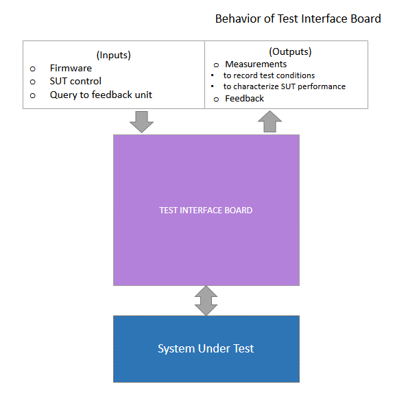
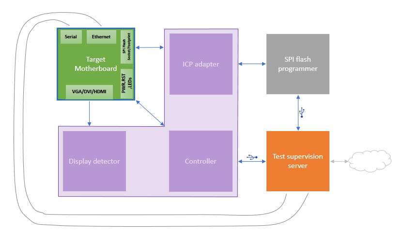
The Test Interface Board provides necessary hardware interface for connecting Test Supervision Server to an SUT. This is necessary to flash firmware to the ROM, to control power/reset sw, to measure PSU voltages and surface temp. of ICs and to take POST feedback if available. Let’s dive into more details to see how this can be done.

Test Interface Board: Detailed box diagrams

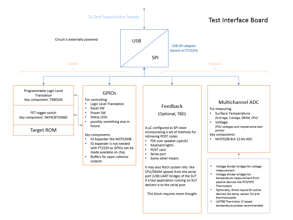
FT232H has a multipurpose serial engine that can be configured as SPI master. FT232H has additional pins that may be used as GPIOs so a GPIO expander may not be needed. The FT232H datasheet states that it offers up to 30mpbs throughput in synchronous serial mode which makes it a fast flashing solution for the given price point (3$). Slave Select (SS) pins can be used to switch between other devices like an ADC that gives voltage and temperature measurements and an optional Feedback microcontroller configured as an SPI slave that gives more information about the SUT. A few GPIO pins can be used to configure Logic Level Translator to ensure compatibility with serial flash of different voltages ranging from 1.8 V to 5V and a GPIO pin will also be used to configure a FET toggle switch (MUX) to electrically detach the serial flash for programming and connecting it back to the motherboard when it’s done.

Notice that I’ve got rid of microcontroller this time. This is because a new microcontroller chip doesn’t necessarily have a bootloader and it needs to be programmed using a dedicated programmer. This adds considerable cost and inconvenience for someone who needs to build only few of these boards. So unless you’re using the optional Feedback module nothing needs to be programmed. Just ordering the board and components and soldering up everything using a 15W iron should be enough to make one of these.

I’m also going to ensure modularity by having small PCBs for each functionality connected to a main-board using headers so that they can be developed independently and used as required. Also, there’s flexibility of choosing temperature probes because it is possible that someone already has good quality probes (that come with professional DMMs).

And a few comments about the ADC I’ve chosen – The ideal choice of ADC for voltage and temperature measurements where the sampling period is large is an integrating ADC. An integrating ADC charges a capacitor from the input signal for a known period of time using an opamp integrator then it discharges that capacitor using a known negative reference voltage. The time it takes to discharge the capacitor is proportional to average value (area under curve) of input signal over sampling period. It’s theoretically simple but it needs use of precision external components and a microcontroller program to work. This is the technique used in professional DMMs (True-RMS) and bench power supplies (for feedback). Delta-Sigma ADCs are common and cheap these days but they don’t average the values over time like integrating ADCs. However, they can provide acceptable accuracy for our application and MCP3208 is a good candidate.

Please see the figure for more details and let me know if there are concerns or suggestions. I’ll post more stuff and schematics in a couple of days.

GSoC (coreboot) Progress till week 2

As you might know my GSoC project is about making a test rig that can make coreboot test systems more accessible to a coreboot test server. This test rig enables coreboot test server to interact with the systems under test (which may be remotely located) in the following ways:

  • Power supply control (discussed in this post)
  • power/reset switch control, voltage and temperature readouts, firmware flashing on serial flash (to be done next)
  • provision for POST feedback (later)

With this project I’m hoping to create an environment where developers will be able to conveniently connect their systems to the coreboot test server for testing at their own place. This is why I like to call it a distributed test environment as it facilitates mass testing without the need to maintain a dedicated testing facility.

So this week I will present a nice and easy solution for power control of the coreboot test systems. I would call this device a ‘programmable power strip’. Before going to the final solution let me first walk you through all the routes that I’ve taken in order to answer some potential questions that may arise. Read on…