GSoC 2013 [flashrom] week #4

There is still no release, but we made quite some progress over the weekend. BSDs should work again as well as Windows (32b) – but the fix for 64b Windows will (most probably) not make it into 0.9.7 because we need to rework a bit of infrastructure code to get this right and we are not too sure about possible breakage from the quick hack I posted. We are still trying to verify the effectiveness of the IMC shutdown patch and looking for Dediprog testers with either an EM100 or a very old flash chip without fast reads. I expect the release to happen in the next two days. Now would be a good time to test flashrom’s trunk or my flashrom_0.9.7 branch on github on flash programmers near you. 😉

I would also welcome contributions to our brain storming about possible features of layout files. I decided to post them to the list instead of making a blog post out of it as envisioned in my last post.

DIY SOIC8 ZIF to DIP8 adapters

As mentioned previously I got an ASRock A180-H sample and want to develop Kabini support for flashrom with it. The board features an 8-pin DIP socket which is way easier to work with than a soldered flash chip, but the included DIP chip is the only one I possess. I do own quite a few SOIC chips though and 3 SOIC8 ZIF sockets though. And one of the two hacker spaces in town has these SOIC8 to DIP8 adapter PCBs in its inventory. So… of course I have built a SOIC8 ZIF to DIP8 adapter out of them.

Complete adapters are usually very expensive (>>50$) for no good reason (from a customer’s perspective only), so building such an adapter is the logical conclusion. Instead of the PCBs from futurlec mentioned above there is a very good deal available from adafruit. The cheapest SOIC ZIF sockets I could find are made by Wieson. They have 3 models available – for “200 mil” 8-pin (G6179-10), “209 mil” 8-pin (G6179-200000) and 16 pin (G6179-070000) chips. They are available from siliconkit (US, 2.5$ per 8-pin adapter, 10 pcs minimum), dediprog (Taiwan, 30$, 15 pcs package), and bios-repair.co.uk (UK, 5£) and probably elsewhere. I am using the G6179-10 below – IMHO the difference of the two 8-pin variants is the length of the chip to be inserted, not its width.

Before acquiring a pre-etched PCB I tried to solder a breakout board myself, similar to this tutorial:

diy_cropped_0

Attaching the wires works somewhat (but one needs steady hands and a lot of patience) but there is one major issue: there is just not enough space to fit the SOIC footprint inside the outline of the DIP pins (the DIP rows of the socket on the mainboard are 0.3″/~8mm apart, the SOIC chip including the pins is about the same size), and of course the pitch is so different that one can’t just solder it on top:
diy_tight_cropped_0

One could try solving this by rotating one of the footprints about 90° and routing the connections manually with enameled wires, but I very much prefer PCBs like this one:
board_cropped_0

Here is the end result with the futurlec PCB which took me a fraction of the time I wrestled with the manual breakout approach:standing_cropped_0

withchip_cropped_0

All pictures above are taken by myself and put into public domain.

GSoC 2013 [flashrom] week #3

After enjoying an extended weekend at the customs office the Micron chips finally arrived at my place and I began testing them with flashrom while preparing parts of this post. One has quite a lot of idle time when testing bigger flash chips with a lousy self-made programmer… the execution of flashrom -w with random data took 52m58s on a 16MB chip (N25Q128) to complete (which is actually two complete reads and one complete erase + read + write cycle per block). Oh if only there would be a cheap but awesome open USB programmer… 😉

Carl-Daniel was still missing till I called him at work yesterday, so Continue reading GSoC 2013 [flashrom] week #3

GSoC [early debugging] Art of refactor

Your branch is ahead of origin/master by 48 commits.

Yes, I knew this would happen, it has become increasingly difficult to push new work for review on gerrit, as I have dependencies  on existing work waiting for merge. As the pile of un-merged patches increases so does the time I spend with git rebase, so I am hoping for some progress on that side.

My eyes in the local working directory have turned towards SerialICE integration inside coreboot tree. The benefits of this approach are better tree structure, wider hardware support, cache-as-ram and usbdebug.

There are several use-cases to consider:

  1. Compile classic stand-alone SerialICE ROM image with ROMCC, using super-IO and chipset initialisation from coreboot tree.
  2. Compile SerialICE as an alternative romstage with ROMCC, using existing coreboot bootblock added with serial port initialisation.
  3. Compile SerialICE as romstage with GCC and cache-as-ram to use existing usbdebug code and possibly better execution performance.
  4. Add abilility to jump out of SerialICE to regular romstage.

Also for the SerialICE session on debug host we have alternatives:

  1. Execute vendor BIOS image under QEMU.
  2. Execute coreboot image under QEMU.
  3. Execute coreboot image in user-mode under GDB without QEMU.
  4. Execute utils like nvramtool, msrtool, inteltool, superiotool, lspci and setpci remotely.

Now all of the above has been demonstrated before but not adopted. Adopting these widely for all mainboards may not happen during my GSoC, as there is no common function to call to enable a serial-port from romstage. At the minimum I will make some simple example one can follow to get SerialICE running on boards with existing coreboot support.


Cooking with thin spaghetti: The hard side of Vultureprog

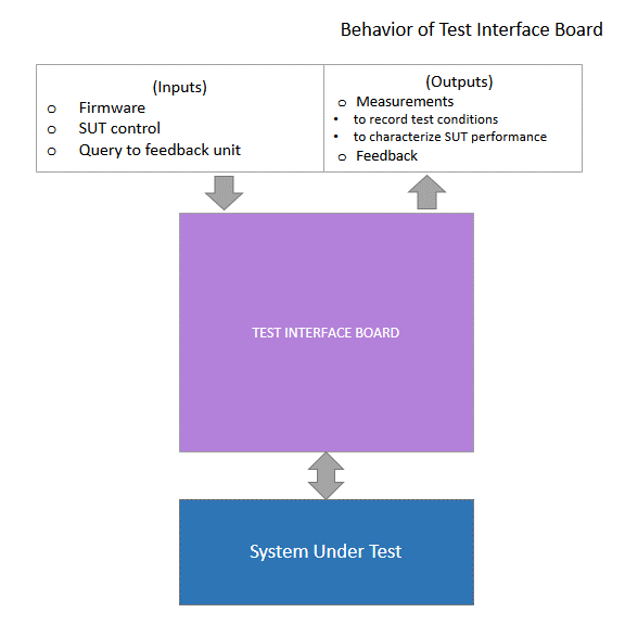
One of the reasons I fell in love with the Stellaris Launchpad boards is that they are modularly vultureprog_3dexpandable. This notion is difficult to explain without comparison to STM Discovery boards, which have a row or two of pins on each side. The idea is simple: you hook one end of your wire to the right pin, and the other end to your breadboard, or you design a custom baseboard specific to the Discovery model. Stellaris takes this idea a little further. The layout of the pins is standardized, not just for the Stellaris, but across the family of TI development boards. Enter the Booster Packs: standardized add-on modules for TI boards. These modules are stackable, so it is possible to connect more than one to a single Stellaris board. This is why I wanted to use the Stellaris for this project. It’s much easier to build a booster pack than to tell people how to connect 32 wires; most people have problems connecting four of them to a buspirate. Let’s look at some of the design choices.

Constraints, constraints, constraints

It’s easy to imagine connecting a LPC chip: six wires and power. In reality, the situation is nowhere near as bright. Four ID pins need to be pulled low, reset pins (yes, there is more than one) need to be pulled high, and some pins simply cannot be left floating. Thus, even a simple bus like LPC becomes a nightmare. Without a logic analyzer to tell what works and what does not, the result is frustration and even self-inflicted injuries. Consequently, I wanted to do a few things right from the beginning(TM).

The most important point was to have all pins properly connected with zero wires. Users should not have to worry about what connects to where. Remember, these chips have 32 pins.

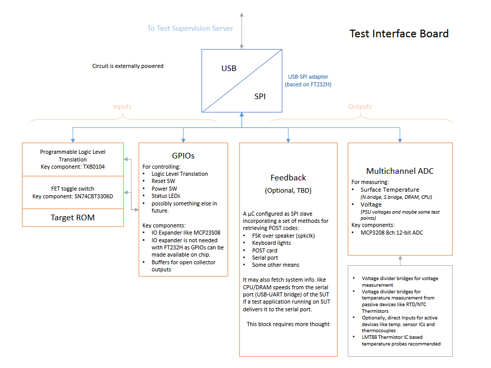
I also wanted to support all possible bus types. LPC and FWH are identical hardware-wise, and are not a problem to support concurrently. SPI is also just a few extra traces that lead to a header. On the other hand, having a programmer that also supports parallel mode is a much harder problem. It turns out there are really two “parallel” modes. The first one is ISA, where the chip is accessed via a linear address space. You put the address you want to access on the address pins, handle a couple of handshake lines to tell the chip if you want to read or write, and move the data over a separate 8-bit data bus.

On the other hand, the second “parallel” mode is a real pain. It uses a 2-dimensional address space, where you need to drive a row address, then a column address, and only then access the data. It’s called PP or “parallel programming” mode. Luckily we get a break: PP mode is an auxiliary programming mode specific to some LPC chips. If we support LPC, we don’t need PP. PP goes in the garbage bin (for now).

Now we need an efficient way to connect the GPIOs to the chip. By “efficient” I mean minimizing the number of GPIO accesses, and the number of bitshifts we need to do in firmware. A poorly chosen pinout will result in abysmal performance, as the 80MHz core struggles to shift the correct bit to the correct GPIO. My choice here was limited, as the best I could do was assign successive GPIOs to successive address pins. I spent the entire Sunday looking over chip datasheets and deciding on this “spaghetti recipe”.

Flexibility – a big issue

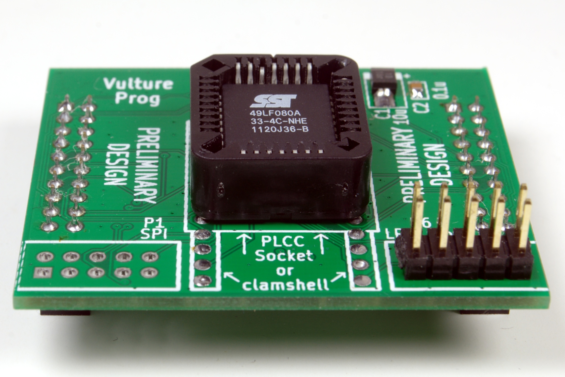
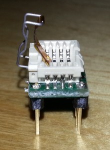
I also wanted to have the option between a normal PLCC32 socket, or a ZIF socket (AKA clamshell). I was really an idiot for thinking I would have both on the same board. On paper, it looks very straightforward. In reality, adjacent pins are on different hemispheres of the globe, and routing them is well, the tastiest spaghetti you have ever eaten. There was no way I could fit both a clamshell, and a PLCC32 socket. There was no way to route the 32 or so tracks on just 2 layers. So I killed the clamshell, the SPI header, and the LPC header. After a couple of hours of messing with the routing, I always had one or two pins that got cornered.

An epic fail

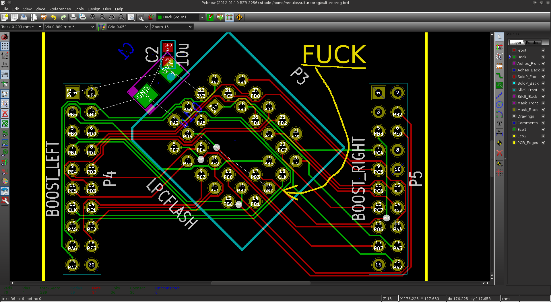
Even routing a simple PLCC socket proved difficult.

What coffee can do to you

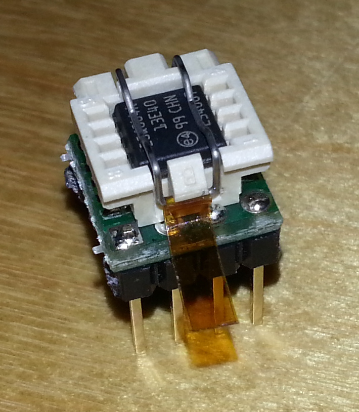
I decided to start over, with all the components in place. Once I reduced the track size to 8 mils, and  spacing to 6 mils, I was able to route two tracks between a set of pins. This time, I placed the socket inside the clamshell, and managed to connect the two using just the top layer. I then worked from the booster pack connection to the DIP pins on the same side of the board, again, using only the top layer. Then I started using the bottom layer for DIP pins on the opposite side. After a few hours, Chuck Norris warped space and time to make room for all the tracks:

A little less epic this time

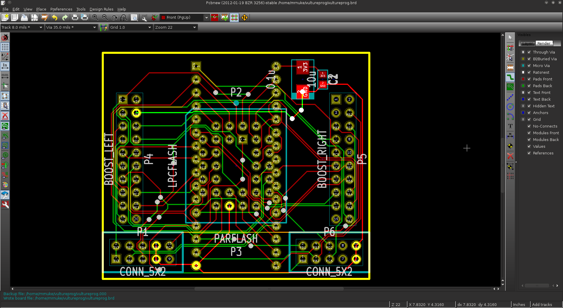
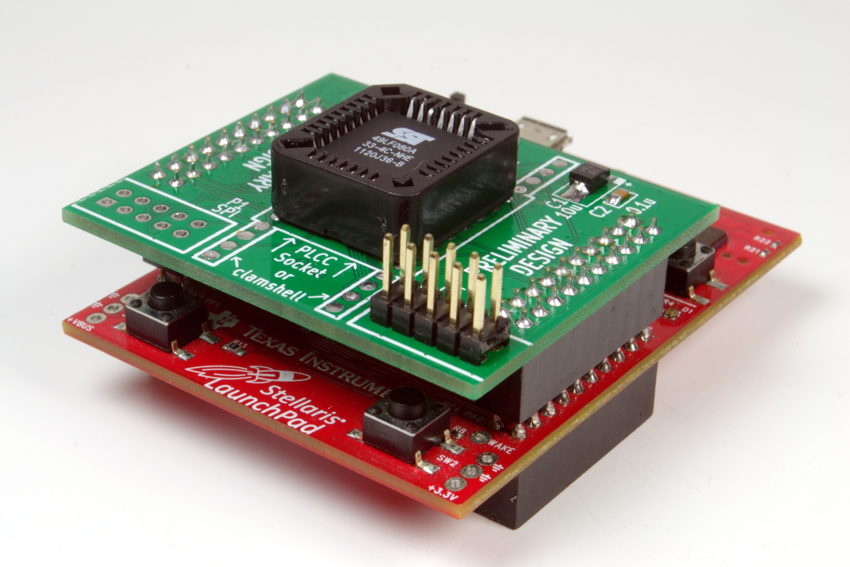
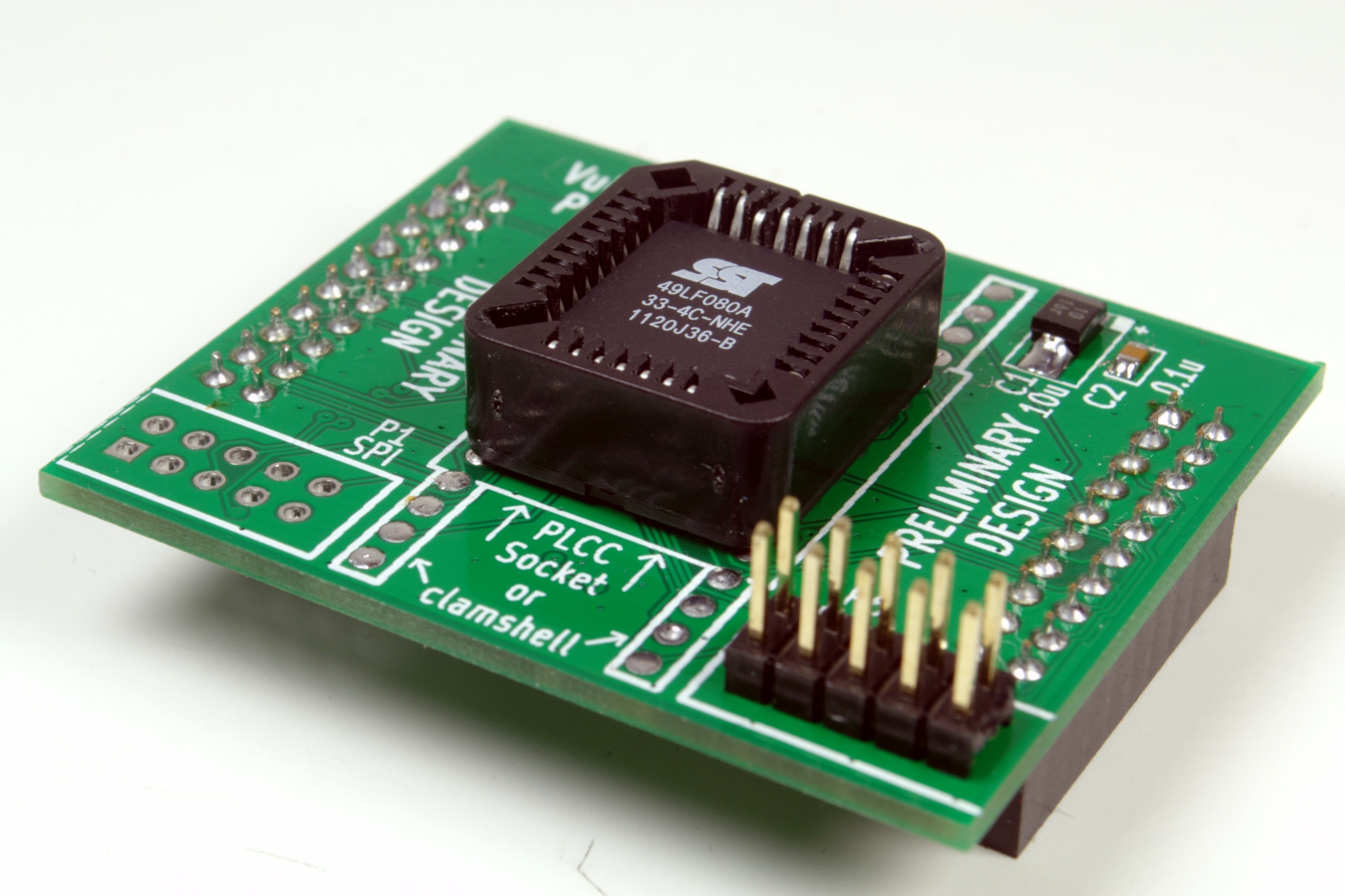
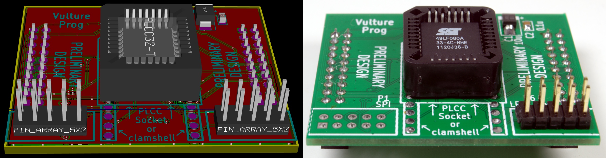
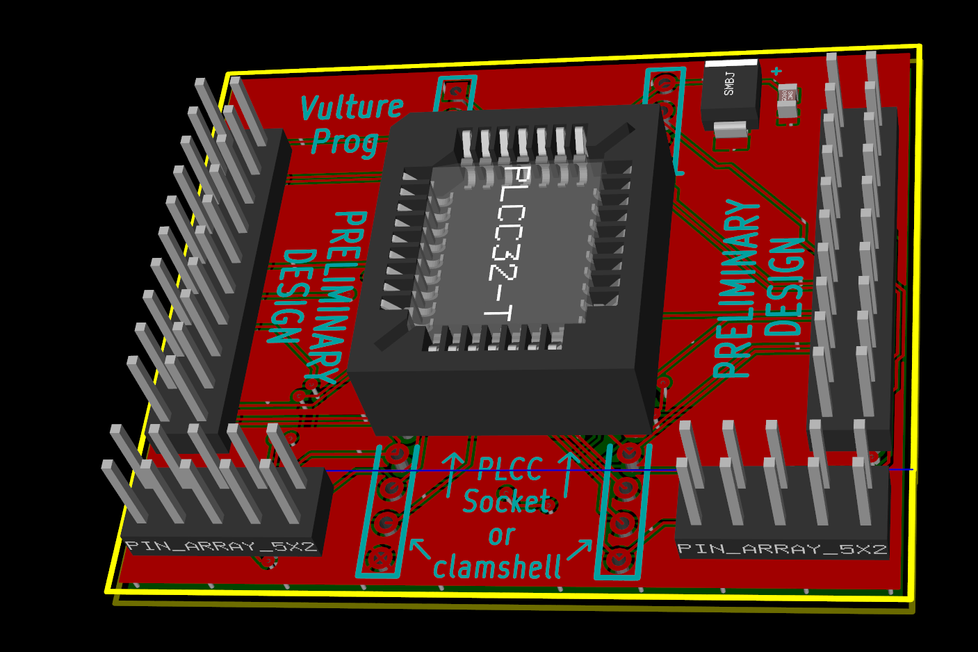
From here, it was a matter of optimizing the routing, taking care of ground planes and other finishing touches. In the end, we get VultureProg hardware version 0.1:

vultureprog_board

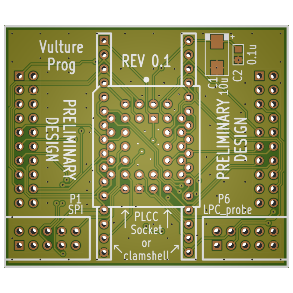
Don’t let the PRELIMINARY DESIGN warning fool you. There is an infinitesimal possibility I will ever want to go back and revise the design. We have 35 GPIOs. accessible on the Stellaris. Five of them are connected to the on-board LEDs and buttons. The remaining 30 are all used up.

Conclusion

If you are a Kicad user, you can head over to yet another one of my GitHub repositories. If you do not have a way to consume Kicad files, you can look in the doc and gerbers directories. Feel free to feed the gerbers to Mayhew Labs’ 3D Gerber Viewer (hint: you can rotate the board in 3D). With all that being done I ordered the first batch of PCBs from Seed Studio’s Fusion PCB service. Routing is definitely too crammed and painful, but I really wanted something versatile and flexible. Whether it lives up to its design goals in REV 0.1 or REV 0.2 remains to be seen. My money is on REV 0.1 — quite literally.

GSoC [coreboot debugging] Now it is broken, now it is not

I feel I did not make much progress the last week, I realised I wasted two days looking for error in my code and I finally found the error elsewhere. As for preparation to push my developments to review, I had rebased my tree. That is, I had picked up the developments done by other people in to my setup. My mistake. While the error still persists there in the master tree, in the process of recovering my platform I learned that there are two types of SOIC-8 SPI flash chips, ones that fit in the miniature socket I have and ones that are physically too large. The spare chips I had were of the second type and that slowed down my system recovery procedure radically. New flash chips are waiting for pickup in the store now.

This is actually just the situation I want coreboot to deal with better in the future: doing a firmware upgrade without the risk of bricking the device to the point where you need to use an external programmer device to recover. Problem is specifically with laptops, which may take a good hour or so to disassemble and put back together, and with every disassembly the risk of breaking some of those miniature connectors increases.

My plan of having two copies of firmware in the same flash chip image just got a bit more complicated. I learned that with recent platforms using a so-called binary blob for raminit, aka. system-agent binary, it is not possible to do a type of dual-boot-prefix setup I had planned, since one cannot put two system-agent binaries in the same CBFS image. I hope the system-agent build and release process is seriously improved to overcome this issue as badly gone(/done) binary blob upgrade procedure was the root-cause of my troubles the past week.

I have not really had a chance to test pre-OS flashing with FILO (actually the code might not yet be available for me to download). Instead I have attacked the low-level PCI and IO sources to reduce a good two or three copies from coreboot tree, this will help my efforts in the long run with SerialICE integration work.


GSoC (coreboot) Progress till week 2

As you might know my GSoC project is about making a test rig that can make coreboot test systems more accessible to a coreboot test server. This test rig enables coreboot test server to interact with the systems under test (which may be remotely located) in the following ways:

  • Power supply control (discussed in this post)
  • power/reset switch control, voltage and temperature readouts, firmware flashing on serial flash (to be done next)
  • provision for POST feedback (later)

With this project I’m hoping to create an environment where developers will be able to conveniently connect their systems to the coreboot test server for testing at their own place. This is why I like to call it a distributed test environment as it facilitates mass testing without the need to maintain a dedicated testing facility.

So this week I will present a nice and easy solution for power control of the coreboot test systems. I would call this device a ‘programmable power strip’. Before going to the final solution let me first walk you through all the routes that I’ve taken in order to answer some potential questions that may arise. Read on…

GSoC 2013 [flashrom] week #2

This week I have a very important directive to share with you:

Working (and especially debugging) in a methodological way does not only mean that every step should be taken on scientific grounds, but that the order of steps should be in an effective order too.

Why do I mention that? Last week I told you that the nice guys at Sage and AMD have sent me an ASRock Kabini board. I received it the following day (which amazed me quite a bit, because it came from US hence it had to undergo a customs check too…), hooked everything up: an old 300W ATX power supply (way overpowered for a 10W SoC) which I have used for coreboot development in the past, USB keyboard and mouse, network, a USB key with Ubuntu and a power button. I switched the PSU on, pressed the button and the fan began to rotate… for a few hundred milliseconds. WTF? I stripped away the non-essential connections and tried again – no change. I thought it could be the PSU – maybe the load is too small or something. But since I had no other supply easily accessible I decided to look at other possible causes: I checked all jumper settings (and there are quite a few of them) and noted a difference between the docs and the actual board regarding the jumpering of an always-on feature (which was a dead end but seemed very promising first), I cleared CMOS memory, reseated the DIMM etc. I even hooked up the flash chip to my logic analyzer to see if it tries to read commands from it… but there was no single proof of life.

So what do you think, is the board dead?

Did you spot the error I made? I hope you did with the blunt hint in the beginning. 🙂 After pulling another PSU out of an old PC and hooking it up everything was fine. *sigh*

When getting the board up eventually I just did a few quick tests (including the flashrom hack that Wei Hu contributed after some discussion in my previous blog post (oh who would have thought that these blog posts are useful at all!? :P)) and put it aside again for hacking in the weeks to come.

The remaining time was spent again on bringing flashrom up to shape for release, waiting for Carl-Daniel and negotiating with a Micron representative over support for their (i.e Numonyx’ and ST’s) chips in flashrom. It has not been the first time for me to mail back and forth with flash vendors, but it is always quite tedious to explain non-technicians and/or people with no idea about open source what we have to offer and what we need; often language barriers play a role too. For example I tried to explain to a Macronix guy about 3 or 4 times why I can not truthfully fill out the sampling order form completely (i.e. the company field) before I gave up. I can’t remember if I filled out the form in the end or not, but I received the samples eventually. Together with the Micron samples that should arrive this week and other samples I received previously I will soon have more than 1GB of SPI flash space at my desk, yay. 🙂

QiProg: The soft side of VultureProg

Another week bites the dust, and coffee supplies are running low. The swarm of zombies is vultureprog_temprestless, but they seem to be active mostly at night. The barricaded windows are holding up well for the time being. I can venture small distances during the day, but not far enough to reach other survivors.  I was able to recover a package from the mailbox this week. Its unannounced appearance is still a mystery, but its contents are most enthralling in this forlorn aeon. I was able to use the waterblocks in the package to reduce my heat signature. There are fewer of THEM trying to break through the barricades. Last night, the leader of the pack did not disturb my hiding place. I don’t know if help will ever come, but I owe it. I owe it to myself, and to the flight engineers. I do not know if they survived, but I owe it to them to finish the flight plans. We must leave this planet.

If you are listening to this transmission, you are a survivor. I have spent this last week in improving the flight plans; I have annotated and documented them in glorious detail. Get them here:

$ git clone git://git.qiprog.org/qiprog.git
$ git clone git://git.qiprog.org/vultureprog.git

 How QiProg works

QiProg was originally designed to be a pure USB protocol, specialized in driving flash chip programmers. Peter Stuge’s original QiProg specification is just that: a USB protocol. But as Peter suggested, once that protocol is converted into API calls, it stops being a protocol, and becomes a full-featured API. It’s amazing how each USB control request can be mapped to one and just one API call. Most USB dependencies become invisible in the API, with a very limited number of exceptions, where the dependence on USB could be inferred from the size of the data structures. Even in these limited cases (hint: there are exactly three), the dependency on the USB bus can trivially be abstracted away. My original reaction was to modify the spec to remove them, but that patch now sits lonely on a forgotten github branch.

QiProg initialization

Initializing the QiProg logic is a very boring boilerplate operation. Luckily, this can be done with just one or two API calls. In fact, I have only included three functions to take care of this. They can create a context, free a context, or set the verbosity of debug messages. That’s it: the very standard boilerplate.

QiProg device discovery

The discovery phase is yet again, boilerplate, albeit a very smart suggestion from Peter. With a single, lightweight call,  qiprog_get_device_list(), QiProg scans all devices and presents them in a flat list. This gives us a bunch of qiprog_device pointer. The qiprog_device pointers are at the heart of QiProg. The public API only presents them as pointers, as opaque as the dictionary allows.

Once we have a device pointer, we can try to open the device, ask the device what it can do, and decide whether or not to hire it. Once we hire a device, the real fun begins

The QiProg core

Remember how I said QiProg devices are presented as opaque pointers? This makes them full-fledged objects. Anytime we want to do anything with the device, we have to perform a device operation. This is exactly where the core come is. It makes sure that the operation is dispatched to the correct handler (more on that later), and makes sure that we don’t crash because of programming mistakes. If I had written QiProg in C++, I would have made the qiprog_device an abstract class, and would have hidden the derived classes and their constructors away from the API.

So, what’s in the core?

qiprog_do_action_x(device, action_parameters...);

That’s about it. action_x can be any of the actions in the original QiProg specification. While it might seem that a _lot_ of logic is needed to make this happen, the core is actually ludicrously lightweight.

Inside the core

QiProg is designed to handle more than just USB programmers. This brings the need for different code paths for each class of devices. Internally, QiProg implements a “driver” for each class. This driver is a structure with function pointers. QiProg asks each of these drivers to scan for available devices, and append them to a context-global device list. This is the exact list we get with qiprog_get_device_list().

So, back to the core. Since the drivers are invisible to the outside world, we can’t get those function pointers. This is the job of the core. The core dereferences the device pointer, and sanity-checks it. This sanity checking removes most boilerplate from the application. And now the magic: each device stores a pointer to its associated driver. All the core has to do is dereference the driver and call the appropriate function with the device as the parameter.

Each device gets a void pointer to store private data. The driver decides what to store there and how to use it. That is sufficient to carry all necessary context information, and why the device pointer is passed to each member of the driver. Since there is no need to look up context information, the core is essentially an O(1) operation. This is the reason we can run the core on the embedded QIProg device.

The hidden QiProg core

Yes, QiProg is running on the VultureProg device as well, not just the host. We don’t care about discovery, or any function that does not need a qiprog_device. Those steps can be handled by standard USB requests; all information is in the USB descriptors. The situation, once again, turns interesting when we have a qiprog_device. VultureProg has a qiprog_device as well (and it can have several).

From USB to the core

Any USB transaction will come in through some sort of hardware-specific channel. It’s the nature of the beast. So, the first thought is: “OK, let’s write a bus IO, hook it into the USB handler, and be done”. However, we can make our USB dispatcher forward control requests to QiProg. And this is where a little file that never seems to be included in the build comes in. qiprog_usb_device.c is never compiled in host code, but is our bridge to QiProg on VultureProg devices. It takes USB requests, and forwards them to a real QiProg driver.

Ok, let’s pause for a second:qiprog_api

Yes, we run QiProg drivers inside the little Cortex-M processor, and with QiProg drivers comes the slick QiProg core. There are a few more tricks we use for making several drivers use the same hardware, but they are far too technical. For the curious, I have to words: “doxygen documented”.

GSoC 2013 [flashrom] week #1: while(1);

This week I was busy preparing flashrom for the 0.9.7 release and queue up some overdue patches to be merged shortly after. This includes the infamous layout patches which I need to polish a bit since quite some time has passed since they were created and the surrounding conditions have changed a bit. Not only did flashrom evolve quite a bit (the original version of the layout patches were part of my GSoC 2011 contributions(!)), but I have learned a few tricks in the meantime too, I hope. Progress is rather slow because I am waiting for Carl-Daniel’s input to various issues but there is no response. That’s also the reason why I chose the subject for this blog post ;).

When I stumbled over a discussion in #coreboot about the new AMD SoCs (Kabini et al, preliminary BKDG), I discovered that they apparently contain a new flash interface supporting all kind of neat stuff (e.g. Multi I/O). This would match parts of my GSoC project perfectly and so I made a joke by asking who will send me a board. To my pleasant and big surprise I received a private message a few minutes later and a brand new ASRock IMB-A180-H is currently on the way to me. I want to express my gratitude to Martin Roth from Sage who was so kind to arrange this and Sage and AMD for paying for it. 🙂

Lately I’ve been looking at libpayload a bit since it will probably play some role in Kyösti’s project in conjunction with libflashrom. So it is also important that I grasp it before I am working on libflashrom. I got (lib)flashrom to compile locally with a slightly patched version of libpayload (patches pushed upstream of course). I hope to get the changes needed in flashrom out before release (NB: I am talking about the current state of libflashrom not about Nico’s patchset). After that I’ll continue to queue up/refine overdue patches – the main focus will be on Nico’s libflashrom.

Kick-starting with some maintenance

EHCI, USB, LOL, OTG, CBMEM, OMG, CAR. Those have been the topics of my first week of GSoC on the coreboot tree. Dozen or so patches in, same amount waiting on approvals or further actions from me. I was glad to find my mentors with many ideas for refactoring and working actively on reviews. Nice start I would say!

It turned out usbdebug support in coreboot may not be very widely tested, hardware has typically had serial ports available for the same task. With some required bugfixes on cache-as-ram and CBMEM, I now have identical output on usbdebug when compared for CBMEM console and serial console. For my setup, that is. More needs to be done to get AMD boards supported once again. I also get to fix usbdebug receive side to make it a usable pipe for GDB and SerialICE, and I want it to handle USB errors and disconnects gracefully.

DIY EHCI debug dongle
USB sandwich with two FX2LP boards.

On the debugging hardware side things have brightened up quite a bit. While the original Net20DC product is discontinued, I was concerned the only solution is the DIY version pictured on the right. I have then received positive feedback and testing from the community (thanks Denis and Aaron) of using some inexpensive ARM boards as USB debug gadgets. To make them work flawlessy, some modification needs to be done on the USB gadget framework drivers on the kernel side. I should try to find someone already familiar with the gadgets to take this development task as I believe it is of interest for kernel developers too.

Some principal decisions on payloads have been made. I would first add usbdebug support for FILO. I am eagerly waiting for the FILO payload with flashrom to be released, this would gain us methods to program the system flashchip from USB storage, in a pre-os environment.